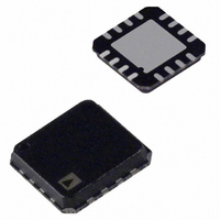
ADXL180WCPZ-RL Analog Devices Inc, ADXL180WCPZ-RL Datasheet - Page 49

ADXL180WCPZ-RL
Manufacturer Part Number
ADXL180WCPZ-RL
Description
IC ACCELEROMETER CONFIG 16-LFCSP
Manufacturer
Analog Devices Inc
Series
iMEMS®r
Datasheet
1.ADXL180WCPZ-RL.pdf
(60 pages)
Specifications of ADXL180WCPZ-RL
Axis
X or Y
Acceleration Range
±50g, 100g, 150g, 200g, 250g, 350g, 500g
Voltage - Supply
5 V ~ 14.5 V
Output Type
Analog
Bandwidth
100Hz ~ 800Hz Selectable
Mounting Type
Surface Mount
Package / Case
16-LFQFN, CSP Exposed Pad
Package Type
LFCSP EP
Operating Supply Voltage (min)
5V
Operating Temperature (min)
-40C
Operating Temperature (max)
125C
Operating Temperature Classification
Automotive
Product Depth (mm)
5mm
Product Height (mm)
1.43mm
Product Length (mm)
5mm
Mounting
Surface Mount
Pin Count
16
Lead Free Status / RoHS Status
Lead free / RoHS Compliant
Sensitivity
-
Interface
-
Lead Free Status / Rohs Status
Compliant
Other names
ADXL180WCPZ-RLCT
CONFIGURATION MODE COMMUNICATIONS
HANDSHAKING
Configuration mode communications uses a handshaking
protocol. Following the completion of a data write or data read
command being written to the ADXL180, a data frame is
transmitted from the ADXL180 through the current mode
serial port. This forms a handshake acknowledgment with the
test system (see Figure 40). The source of the data (RAM or
OTP) transmitted in the handshake data frame is dependent
on whether the OTP memory has been programmed.
Upon receiving a configuration mode data frame, if a parity
error is detected, the ADXL180 returns a handshake data frame
with the state vector code set to the status/error state vector
code (110b). The 8-bit data field and the 4-bit address field are
both set to all 0s.
When the test system sends a data write command, the data that
was written to the addressed configuration mode register is then
I
V
BUS
BP
HANDSHAKE
DATA WRITE
Figure 40. Configuration Mode Write Data and Read Data Sequences
DATA WRITE SEQUENCE
t
tm1
TRANSMIT
DATA
Rev. A | Page 49 of 60
t
tm2
TIME
HANDSHAKE
DATA READ
written to RAM, read back from the RAM, and transmitted to
the user’s test/configuration system as a handshake. This provides
a data integrity check for data write commands. If there is an
attempt to write data to a RAM register after the CUPRG bit is
set, the data is ignored by the ADXL180 (that is, it has no affect
on the device). The data returned by the ADXL180 is the
contents of the addressed OTP fuse register. This is the same
result as if a data read command had been issued.
When the test/configuration system sends a data read command,
the data contained in the data frame is ignored and the data that
is contained in the addressed configuration mode register is
sent to the test/configuration system in response. The data sent
is always read from the RAM registers. If the CUPRG bit has
not been set (that is, the OTP fuses are not programmed), the
RAM contains the last data written to it by the configuration/
test system. When the CUPRG bit is set (that is, the OTP fuses
are programmed) the fuse data is loaded into the RAM registers
(see Figure 42).
DATA READ SEQUENCE
t
tm1
TRANSMIT
DATA
t
tm2
ADXL180


