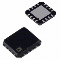
ADXL180WCPZ-RL Analog Devices Inc, ADXL180WCPZ-RL Datasheet - Page 53

ADXL180WCPZ-RL
Manufacturer Part Number
ADXL180WCPZ-RL
Description
IC ACCELEROMETER CONFIG 16-LFCSP
Manufacturer
Analog Devices Inc
Series
iMEMS®r
Datasheet
1.ADXL180WCPZ-RL.pdf
(60 pages)
Specifications of ADXL180WCPZ-RL
Axis
X or Y
Acceleration Range
±50g, 100g, 150g, 200g, 250g, 350g, 500g
Voltage - Supply
5 V ~ 14.5 V
Output Type
Analog
Bandwidth
100Hz ~ 800Hz Selectable
Mounting Type
Surface Mount
Package / Case
16-LFQFN, CSP Exposed Pad
Package Type
LFCSP EP
Operating Supply Voltage (min)
5V
Operating Temperature (min)
-40C
Operating Temperature (max)
125C
Operating Temperature Classification
Automotive
Product Depth (mm)
5mm
Product Height (mm)
1.43mm
Product Length (mm)
5mm
Mounting
Surface Mount
Pin Count
16
Lead Free Status / RoHS Status
Lead free / RoHS Compliant
Sensitivity
-
Interface
-
Lead Free Status / Rohs Status
Compliant
Other names
ADXL180WCPZ-RLCT
0
1
0
1
UD[7:0] USER DATA BITS
The user register is for arbitrary user data. It does not have any
influence on sensor operation. This data is transmitted during
Phase 2 of the state machine. For more information on trans-
mission format and timing, in particular depending on the
setting of MD bits, see the ADXL180 State Machine section.
Table 45. User Data Bit Definitions
Bit
Names
UD0
UD1
UD2
UD3
UD4
UD5
UD6
UD7
UD8 CONFIGURATION BIT
Table 46. UD8 Configuration Bit
UD8
0
1
The value of the RS bit may be transmitted during Phase 2, inde-
pendent of UD[7:0], depending on the selection of the MD bits.
BDE
Table 47. Bus Discharge Enable
BDE
The bus discharge enable (BDE) bit enables a discharge of the
bus voltage after a synchronization pulse is detected. If the BDE
bit is set, the ADXL180 changes the bus current (I
I
See the Synchronous Communication section for more details
and timing information.
SCOE
Table 48. SCOE V
SCOE
IDLE
to I
Bus discharge disabled (default).
Bus discharge enabled. Only active when SYEN = 1.
Definition
SIG
V
V
conversion is present on V
impedance input or data or sensor data may be
adversely affected.
Definition
SCO
SCO
Definition
User Data Bit 0. No function, data only.
User Data Bit 1. No function, data only.
User Data Bit 2. No function, data only.
User Data Bit 3. No function, data only.
User Data Bit 4. No function, data only.
User Data Bit 5. No function, data only.
User Data Bit 6. No function, data only.
User Data Bit 7. No function, data only.
when a valid synchronization pulse has been detected.
output disabled. (Default.)
output enabled. Analog output prior to ADC
Definition
Reserved, don’t care (default)
Reserved, don’t care
SCO
Signal Chain Output Enable
SCO
pin. Connect V
BUS
SCO
) level from
to high
Rev. A | Page 53 of 60
FDLY
Table 49. Fixed Delay Mode
FDLY
0
1
ADME
Table 50. Autodelay Mode Enable (ADME ) Options
ADME
0
1
STI
Table 51. Self Test Internal (STI) Options
STI
0
1
Table 52. Phase 3 Data Transmitted When STI = 1
MD1
0
0
1
1
FC[1:0]
Table 53. FC Low-Pass Filter Bandwidth Frequency Select Codes
FC1
0
0
1
1
RG[2:0]
Table 54. RG[2:0] Sensor Range Select Codes
RG2
0
0
0
0
1
1
1
1
External self-test. User must monitor self-test data to
verify proper operation. Device does not monitor its own
response to the self-test stimulus. (Default.)
Internal self-test. The device monitors its own self-test
data to determine proper operation.
Definition
Fixed delay mode disabled (default).
Fixed delay mode enabled. Device transmits data in the
time slot delayed by t
Definition
MD0
0
1
0
1
Definition
Autodelay mode disabled. The part does not check for
a second device on the line and does not pull any extra
current during startup. (Default.)
Autodelay mode detection enabled. I
6 ms at power-up.
FC0
0
1
0
1
0
0
1
1
0
0
1
1
RG1
Data
Device OK
Range
Delimiter
Device OK
−3 dB LP Frequency
400 Hz
200 Hz
100 Hz
800 Hz
RG0
0
1
0
1
0
1
0
1
DLY
as defined by DLY[2:0].
Range
±50 g
±100 g
±250 g
±150 g
±200 g
±350 g
±500 g
Not used
DET
pull-down for
ADXL180


