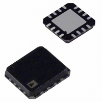
ADXL180WCPZ-RL Analog Devices Inc, ADXL180WCPZ-RL Datasheet - Page 48

ADXL180WCPZ-RL
Manufacturer Part Number
ADXL180WCPZ-RL
Description
IC ACCELEROMETER CONFIG 16-LFCSP
Manufacturer
Analog Devices Inc
Series
iMEMS®r
Datasheet
1.ADXL180WCPZ-RL.pdf
(60 pages)
Specifications of ADXL180WCPZ-RL
Axis
X or Y
Acceleration Range
±50g, 100g, 150g, 200g, 250g, 350g, 500g
Voltage - Supply
5 V ~ 14.5 V
Output Type
Analog
Bandwidth
100Hz ~ 800Hz Selectable
Mounting Type
Surface Mount
Package / Case
16-LFQFN, CSP Exposed Pad
Package Type
LFCSP EP
Operating Supply Voltage (min)
5V
Operating Temperature (min)
-40C
Operating Temperature (max)
125C
Operating Temperature Classification
Automotive
Product Depth (mm)
5mm
Product Height (mm)
1.43mm
Product Length (mm)
5mm
Mounting
Surface Mount
Pin Count
16
Lead Free Status / RoHS Status
Lead free / RoHS Compliant
Sensitivity
-
Interface
-
Lead Free Status / Rohs Status
Compliant
Other names
ADXL180WCPZ-RLCT
ADXL180
CONFIGURATION MODE COMMAND (RECEIVE)
COMMUNICATIONS PROTOCOL
The 8-bit configuration register data is passed to the ADXL180
with a read/write command bit, a 4-bit configuration register
address, and a parity bit as shown in Figure 39. The read/write
bit is set to indicate the desired action. A 0 indicates a write
Table 42. Configuration Mode Transmit Data Bit Mapping
DB15
Parity
DB14
Addr 3
DB13
Addr 2
DB12
Addr 1
TRANSMITTED
DB11
Addr 0
FIRST
Figure 39. Configuration Mode Command (Receive) Data Frame
DB10
Data
Bit 7
(MSB)
0
1
DB9
Data
Bit 6
2
Rev. A | Page 48 of 60
3
DATA
DB8
Data
Bit 5
RECEIVE DATA FRAME (14 BITS)
4
5
DB7
Data
Bit 4
6
operation and a 1 indicates a read operation. The parity bit is set
for even parity. The parity bit should be set to 0 or 1 to make the
total number of 1s in the data frame even. The data is
transmitted LSB first as shown in Table 42.
7
DB6
Data
Bit 3
0
ADDRESS
1
DB5
Data
Bit 2
2
3
DB4
Data
Bit 1
R/W
0
P
0
DB3
Data
Bit 0
(LSB)
DB2
State
Vector 2
DB1
State
Vector 1
DB0
State
Vector 0


