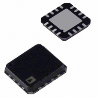
ADXL180WCPZ-RL Analog Devices Inc, ADXL180WCPZ-RL Datasheet - Page 46

ADXL180WCPZ-RL
Manufacturer Part Number
ADXL180WCPZ-RL
Description
IC ACCELEROMETER CONFIG 16-LFCSP
Manufacturer
Analog Devices Inc
Series
iMEMS®r
Datasheet
1.ADXL180WCPZ-RL.pdf
(60 pages)
Specifications of ADXL180WCPZ-RL
Axis
X or Y
Acceleration Range
±50g, 100g, 150g, 200g, 250g, 350g, 500g
Voltage - Supply
5 V ~ 14.5 V
Output Type
Analog
Bandwidth
100Hz ~ 800Hz Selectable
Mounting Type
Surface Mount
Package / Case
16-LFQFN, CSP Exposed Pad
Package Type
LFCSP EP
Operating Supply Voltage (min)
5V
Operating Temperature (min)
-40C
Operating Temperature (max)
125C
Operating Temperature Classification
Automotive
Product Depth (mm)
5mm
Product Height (mm)
1.43mm
Product Length (mm)
5mm
Mounting
Surface Mount
Pin Count
16
Lead Free Status / RoHS Status
Lead free / RoHS Compliant
Sensitivity
-
Interface
-
Lead Free Status / Rohs Status
Compliant
Other names
ADXL180WCPZ-RLCT
ADXL180
CONFIGURATION SPECIFICATION
OVERVIEW
The ADXL180 configuration mode allows access to the user-
programmable nonvolatile configuration registers used to
define the function of the device. The configuration mode is
entered by writing a 16-bit configuration mode enable key code
to the V
which begins immediately after power is applied to the ADXL180.
The 16-bit configuration mode enable key code is 0x5A5A with
no start or parity bits (see Figure 36). The configuration mode
key is sent LSB first. Note that the configuration mode key code
is 16 bits long and the configuration mode read/write command
data frames are 14 bits long. This helps avoid misinterpretation
of either by the ADXL180.
All configuration mode data sent to the ADXL180, including
the configuration mode enable key code is communicated to
BP
pin during Phase 1 of the ADXL180 start-up sequence,
CLOCK
DATA
V
V
I
BP
CT
V
BUS
BP
TRANSMITTED
Figure 35. Configuration Mode Receive Pulse Width Data and Clock Encoding
16-BIT CONFIG MODE KEY CODE
FIRST
Figure 36. Configuration Mode Enable Key Code Data Frame
0
Figure 37. Configuration Mode Entry Key Code Sequence
1
CONFIGURATION MODE ENABLE KEY DATA FRAME (16 BITS)
0
1
t
IB
Rev. A | Page 46 of 60
1
t
CONFIGURATION MODE KEY
PGO
0
TIME
t
0
IB
1
TIME
t
tm1
0
the ADXL180 via voltage modulation of the V
respect to the V
tion to combine the clock and digital data. The clock and data
are encoded as shown in Figure 35.
The ADXL180 acknowledges entering the configuration mode
by transmitting the contents of the CREG2 register. This register
contains the configuration/user data programming bit (CUPRG)
status. This allows the user’s configuration/test system to deter-
mine whether the ADXL180 configuration OTP fuse memory
has been programmed without further communication. If the
configuration mode is not entered within the Phase 1 initializa-
tion time period, the ADXL180 treats the pulses on the V
as synchronization pulses (in synchronous mode) or ignores
them in asynchronous mode.
t
PG1
0
18-BIT TRANSMIT DATA:
1
t
1
IB
0
CREG2
1
BN
t
PG1
1
pin. This signal uses pulse duration modula-
0
t
1
IB
1
t
t
PG0
0
tm2
t
0
IB
BP
pin with
BP
pin


