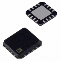
ADXL180WCPZ-RL Analog Devices Inc, ADXL180WCPZ-RL Datasheet - Page 50

ADXL180WCPZ-RL
Manufacturer Part Number
ADXL180WCPZ-RL
Description
IC ACCELEROMETER CONFIG 16-LFCSP
Manufacturer
Analog Devices Inc
Series
iMEMS®r
Datasheet
1.ADXL180WCPZ-RL.pdf
(60 pages)
Specifications of ADXL180WCPZ-RL
Axis
X or Y
Acceleration Range
±50g, 100g, 150g, 200g, 250g, 350g, 500g
Voltage - Supply
5 V ~ 14.5 V
Output Type
Analog
Bandwidth
100Hz ~ 800Hz Selectable
Mounting Type
Surface Mount
Package / Case
16-LFQFN, CSP Exposed Pad
Package Type
LFCSP EP
Operating Supply Voltage (min)
5V
Operating Temperature (min)
-40C
Operating Temperature (max)
125C
Operating Temperature Classification
Automotive
Product Depth (mm)
5mm
Product Height (mm)
1.43mm
Product Length (mm)
5mm
Mounting
Surface Mount
Pin Count
16
Lead Free Status / RoHS Status
Lead free / RoHS Compliant
Sensitivity
-
Interface
-
Lead Free Status / Rohs Status
Compliant
Other names
ADXL180WCPZ-RLCT
ADXL180
CONFIGURATION AND USER DATA REGISTERS
The configuration and user data registers are the user register,
UREG, and the three configuration registers, CREG0, CREG1,
and CREG2 (see Table 44). The ADXL180 can be programmed
to provide a variety of signal chain characteristics and device
operating modes via Configuration Register CREG0, Configu-
ration Register CREG1, and Configuration Register CREG2.
The configuration register and user register data can be
programmed into nonvolatile OTP memory.
In general, the CREG registers hold data that alters the function
of the ADXL180. The data contained in the UREG has no affect
on the operation of the ADXL180. The UREG bits are typically
used to indicate information such as module housing type and
sensing axis. The ADXL180 can be programmed to transmit the
UREG bits as part of the device data during power-up Phase 2,
depending on the Phase 2 mode that is selected.
CONFIGURATION MODE EXIT
The configuration mode is exited by writing 0x80 to
Address 1010b. A communication handshake is transmitted
by the ADXL180 after the configuration mode exit address is
written. The ADXL180 reenters its start-up sequence at the
beginning of the initialization phase (Phase 1) immediately
upon exiting the configuration mode. This method does not
generate a device reset. Alternatively, the configuration mode
can be exited by lowering the bus supply voltage to cause a
power-on-reset to occur. This method generates a device reset.
SERIAL NUMBER AND MANUFACTURER
IDENTIFICATION DATA REGISTERS
The serial number and manufacturer identification data
registers can be read in configuration mode. The manufacturer
identification register is fixed at the mask level. The serial
number is programmed during the final manufacturing stages.
I
V
BUS
V
BP
DD
CONFIGURATION
SEQUENCE
MODE KEY
WRITE
UREG
DATA
SEQ
Figure 41. Example Configuration Register OTP Programming Sequence
CREG0
WRITE
DATA
SEQ
CREG1
WRITE
DATA
SEQ
Rev. A | Page 50 of 60
TIME
CREG2
WRITE
DATA
SEQ
The ADXL180 can be configured to send this data as part of the
device data transmitted during Phase 2 of the power-up
initialization sequence.
PROGRAMMING THE CONFIGURATION AND USER
DATA REGISTERS
When the desired configuration and user data has been written
to the UREG and CREG registers, writing a 1 to the configura-
tion/user data program command bit (CUPRG) causes the four
bytes of configuration/user data to be permanently written to
the configuration/user data OTP fuse memory. The OTP fuses
are programmed sequentially by the ADXL180 without further
user intervention. This takes about 12 ms (t
The ADXL180 ignores all test system read and write commands
while it is programming the fuses.
The ADXL180 acknowledges the completion of the program-
ming sequence of the configuration/user data OTP memory by
sending the contents of the CREG2 register as described in the
Configuration Mode Transmit Communications Protocol section.
The CREG2 register contains the configuration/user data pro-
gramming bit (CUPRG). This allows the test/configuration
system to verify that the configuration/user data programming
bit has been programmed without further communication. The
contents of all of the configuration and user registers should then
be read to confirm that they have been programmed to the desired
settings. Figure 41 illustrates a sample sequence of commands
to write and then program the configuration and user registers.
Once programmed, the OTP fuse memory settings are loaded
into the RAM registers during the Phase 1 initialization of the
ADXL180 start-up sequence. Figure 42 shows the basic struc-
ture of the configuration and user RAM/OTP memory structure.
REGISTER OTP PROGRAMMING
INTERNAL CONFIGURATION
SEQUENCE
t
CUP
DATA
WRITE
EXIT
CM
CREG2
HANDSHAKE
CUP
in Figure 41).


