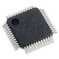
OX16C950-TQBG OXFORD SEMICONDUCTOR, OX16C950-TQBG Datasheet - Page 12

OX16C950-TQBG
Manufacturer Part Number
OX16C950-TQBG
Description
IC, UART, 1CH, SMD, TQFP48, 950
Manufacturer
OXFORD SEMICONDUCTOR
Datasheet
1.OX16C950-TQBG.pdf
(50 pages)
Specifications of OX16C950-TQBG
No. Of Channels
1
Data Rate
15Mbps
Uart Features
Tx/Rx FIFO INT TRIG
Supply Voltage Range
3V To 5.25V
Operating Temperature Range
0°C To +70°C
Digital Ic Case Style
TQFP
No. Of Pins
48
Lead Free Status / RoHS Status
Lead free / RoHS Compliant
Available stocks
Company
Part Number
Manufacturer
Quantity
Price
Company:
Part Number:
OX16C950-TQBG
Manufacturer:
SAMSUNG
Quantity:
450
4.1
Pin
CS0
CS1
CS2#
IOR
IOW
INTSEL# Interrupt Control Mode
RXRDY# DMA Control signal output
TXRDY# DMA Control signal output
BDOUT# Baud rate generator output
RCLK
XTLI
XTLO
DDIS
ADS#
OUT1#
OUT2#
SOUT
SIN
RTS#
CTS#
DTR#
DSR#
DS-0031 Sep 05
OXFORD SEMICONDUCTOR LTD.
Further Pin Information
Description
Chip Select
Chip Select
Chip Select
Additional I/O Read Control
Additional I/O Write Control
Receiver clock input
Crystal circuit input
Crystal circuit output
Driver Disable output
Address Strobe In
User defined output
User defined output
Serial data output
Serial data input
Request-To-Send Modem
signal output
Clear-To-Send Modem signal
input
Data-Terminal-Ready
Modem signal output
Data-Set-Ready
Modem signal input
Action when used
Connect to active high chip select generation
logic
Connect to active high chip select generation
logic
Connect to active low chip select generation
logic
Connect to processors active high I/O read
line (and tie IOR# high)
Connect to processors active high I/O write
line (and tie IOW# high)
Tie low to allow software enable/disable of the
interrupt pin.
Connect direct to DMA control circuitry
Connect direct to DMA control circuitry
Connect direct to the RCLK pin in order to run
the receiver with the same clock as the
transmitter
Connect directly to a suitable receiver clock
source (Usually the BDOUT# pin)
Connect to suitable clock input
Connect to crystal oscillator circuit
Connect to active high bus transceiver drive
disable (goes high when device is not being
read from)
Connect direct to external control circuitry
(Low-High transition on this pin latches CS0-2
and A0-2)
Connect direct to TTL input of external circuit
to control
Connect direct to TTL input of external circuit
to control
Connect to a suitable line driver
Connect to a suitable line driver
Connect to a suitable line receiver
Connect to a suitable line driver
Connect to a suitable line receiver
Connect to a suitable line receiver
Common Channel Pins
Miscellaneous Pins
Clock Related Pins
Bus Interface Pins
External—Free Release
Control Pins
DMA Pins
Action when not used
Tie high – All chip selects must be
active in order to access the device
Tie high – All chip selects must be
active in order to access the device
Tie low – All chip selects must be active
in order to access the device
Tie low (IOR# will be used to control I/O
read operations)
Tie low (IOW# will be used to control
I/O read operations)
Leave unconnected (Pulled high
internally to leave the interrupt pin
permanently enabled).
Leave unconnected
Leave unconnected
Leave unconnected
Leave unconnected
Leave unconnected
Tie low
Leave unconnected
Leave unconnected
Leave unconnected
(Serial data can not be transmitted)
Leave unconnected
(Serial data can not be received)
Leave unconnected
Tie high
Leave unconnected
Tie high
OX16C950 rev B
n/a
n/a
Page 12


