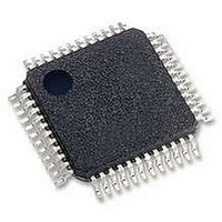
OX16C950-TQBG OXFORD SEMICONDUCTOR, OX16C950-TQBG Datasheet - Page 37

OX16C950-TQBG
Manufacturer Part Number
OX16C950-TQBG
Description
IC, UART, 1CH, SMD, TQFP48, 950
Manufacturer
OXFORD SEMICONDUCTOR
Datasheet
1.OX16C950-TQBG.pdf
(50 pages)
Specifications of OX16C950-TQBG
No. Of Channels
1
Data Rate
15Mbps
Uart Features
Tx/Rx FIFO INT TRIG
Supply Voltage Range
3V To 5.25V
Operating Temperature Range
0°C To +70°C
Digital Ic Case Style
TQFP
No. Of Pins
48
Lead Free Status / RoHS Status
Lead free / RoHS Compliant
Available stocks
Company
Part Number
Manufacturer
Quantity
Price
Company:
Part Number:
OX16C950-TQBG
Manufacturer:
SAMSUNG
Quantity:
450
15.4
The TTL register is located at offset 0x04 of the ICR
Whenever 950 trigger levels are enabled (ACR[5]=1), bits 4
and 5 of FCR are ignored and an alternative arbitrary
transmitter interrupt trigger level can be defined in the TTL
register. This 7-bit value provides a fully programmable
transmitter interrupt trigger facility. In 950 mode, a priority
level 3 interrupt occurs indicating that the transmitter buffer
requires more characters when the interrupt is not masked
(IER[1]=1) and the transmitter FIFO level falls below the
value stored in the TTL register. The value 0 (0x00) has a
special meaning. In 950 mode when the user writes 0x00
to the TTL register, a level 3 interrupt only occurs when the
FIFO and the transmitter shift register are both empty and
the SOUT line is in the idle marking state. This feature is
particularly useful to report back the empty state of the
transmitter after its FIFO has been flushed away.
15.5
The RTL register is located at offset 0x05 of the ICR
Whenever 950 trigger levels are enabled (ACR[5]=1), bits 6
and 7 of FCR are ignored and an alternative arbitrary
receiver interrupt trigger level can be defined in the RTL
register. This 7-bit value provides a fully programmable
receiver interrupt trigger facility as opposed to the limited
trigger levels available in 16C650 and 16C750 devices. It
enables the system designer to optimise the interrupt
performance hence minimising the interrupt overhead.
In 950 mode, a priority level 2 interrupt occurs indicating
that the receiver data is available when the interrupt is not
masked (IER[0]=1) and the receiver FIFO level reaches the
value stored in this register.
15.6
The FCL and FCH registers are located at offsets 0x06 and
0x07 of the ICR respectively
Enhanced software flow control using XON/XOFF and
hardware flow control using RTS#/CTS# and DTR#/DSR#
are available when 950 mode trigger levels are enabled
(ACR[5]=1). Improved flow control threshold levels are
offered using Flow Control Lower trigger level (‘FCL’) and
Flow Control Higher trigger level (‘FCH’) registers to
provide a greater degree of flexibility when optimising the
flow control performance. Generally, these facilities are
only available in Enhanced mode.
In 650 mode, in-band flow control is enabled using the EFR
register. An XOFF character is transmitted when the
DS-0031 Sep 05
OXFORD SEMICONDUCTOR LTD.
Transmitter Trigger Level ‘TTL’
Receiver Interrupt. Trigger Level ‘RTL’
Flow Control Levels ‘FCL & FCH’
External—Free Release
receiver FIFO exceeds the upper trigger level defined by
FCR[7:6] as described in section 8.1. An XON is then sent
when the FIFO is read down to the lower fill level. The flow
control is enabled and the appropriate mode selected using
EFR[3:0].
In 950 mode, the flow control thresholds defined by
FCR[7:6] are ignored. In this mode threshold levels are
programmed using FCL and FCH. When in-band flow
control is enabled (defined by EFR[3:0]) and the receiver
FIFO level (‘RFL’) reaches the value programmed in the
FCH register, an XOFF is transmitted to stop the flow of
serial data . The flow is resumed when the receiver FIFO
fill level falls to below the value programmed in the FCL
register, at which point an XON character is sent. The FCL
value of 0x00 is illegal.
For example if FCL and FCH contain 64 and 100
respectively, XOFF is transmitted when the receiver FIFO
contains 100 characters, and XON is transmitted when
sufficient characters are read from the receiver FIFO such
that there are 63 characters remaining.
CTS/RTS and DSR/DTR out-of-band flow control use the
same trigger levels as in-band flow control. When out-of-
band flow control is enabled, RTS# (or DTR#) line is de-
asserted when the receiver FIFO level reaches the upper
limit defined in the FCH and is re-asserted when the
receiver FIFO is drained below the lower limit defined in
FCL. When 950 trigger levels are enabled (ACR[5]=1), the
CTS# flow control functions as in 650 mode and is
configured by EFR[7]. However, when EFR[6] is set, RTS#
is automatically de-asserted when RFL reaches FCH and
re-asserted when RFL drops below FCL.
DSR# flow control is configured with ACR[2]. DTR# flow
control is configured with ACR[4:3].
15.7
The identification registers is located at offsets 0x08 to 0x0B
of the ICR
The OX16C950 offers four bytes of device identification.
The device ID registers may be read using offset values
0x08 to 0x0B of the Indexed Control Register. Registers
ID1, ID2 and ID3 identify the device as an OX16C950 and
return 0x16, 0xC9 and 0x50 respectively. The REV register
resides at offset 0x0B of ICR and identifies the revision of
950 core. This register returns 0x03 for revision B of the
OX16C950.
Device Identification Registers
OX16C950 rev B
Page 37


