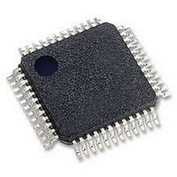
OX16C950-TQBG OXFORD SEMICONDUCTOR, OX16C950-TQBG Datasheet - Page 44

OX16C950-TQBG
Manufacturer Part Number
OX16C950-TQBG
Description
IC, UART, 1CH, SMD, TQFP48, 950
Manufacturer
OXFORD SEMICONDUCTOR
Datasheet
1.OX16C950-TQBG.pdf
(50 pages)
Specifications of OX16C950-TQBG
No. Of Channels
1
Data Rate
15Mbps
Uart Features
Tx/Rx FIFO INT TRIG
Supply Voltage Range
3V To 5.25V
Operating Temperature Range
0°C To +70°C
Digital Ic Case Style
TQFP
No. Of Pins
48
Lead Free Status / RoHS Status
Lead free / RoHS Compliant
Available stocks
Company
Part Number
Manufacturer
Quantity
Price
Company:
Part Number:
OX16C950-TQBG
Manufacturer:
SAMSUNG
Quantity:
450
18.2
N.B. Maximum frequency of operation is downgraded under 3V operation to 50 MHz.
Note 1:
Note 2:
Note 3:
Note 4:
DS-0031 Sep 05
OXFORD SEMICONDUCTOR LTD.
3V Operation
t
ADS# signal may be tied low if address is stable during read or write cycles.
t
In Isochronous mode, transmitter data is available after the falling edge of the x1 clock and the receiver data is sampled using the
rising edge of the x1 clock. The system designer is should ensure that mark-to-space ratio of the x1 clock is such that the required
set-up and hold timing constraint are met. One way of achieving this is to choose a crystal frequency which is twice the required data
rate and then divide the clock by two using the on-board prescaler. In this case the mark-to-space ratio is 50/50 for the purpose of
set-up and hold calculations.
ha
had,
and t
t
a1
Symbol
and t
hc
t
t
t
t
t
t
t
t
t
t
t
t
t
t
t
t
t
t
acc
t
sac
hac
had
w1
w2
sa
ha
hc
sd
hd
a1
irs
irh
sc
r1
r2
df
its
timing constrains only apply to non-multiplexed arrangement where ADS# is permanently tied low.
sac
timing constrains only apply to multiplexed arrangement where ADS# is used.
Parameter
Address set-up time to IOR# or IOW# falling
Address set-up time to IOR or IOW rising
Address hold time after IOR# or IOW# rising
Address hold time after IOR or IOW falling
Chip select set-up time to IOR# or IOW# falling
Chip select set-up time to IOR or IOW rising
Chip select hold time after IOR# or IOW# rising
Chip select hold time after IOR or IOW falling
Pulse duration of IOR# or IOR
Delay between IOR# rising and IOR#/IOW# falling
Delay between IOR falling and IOR/IOW rising
Access time; Data valid after IOR# falling or IOR rising
Data bus floating after IOR# rising or IOR rising
Pulse duration of IOW# or IOW
Delay between IOW# rising and IOR# /IOW# falling
Delay between IOW falling and IOR/IOW rising
Data set-up time to IOW# rising or IOW falling
Data hold time after IOW# rising or IOW falling
Address and chip select set-up time to ADS#
rising
Address and chip select hold time after ADS#
rising
Pulse duration of ADS#
IOR#/IOW# rising or IOR/IOW falling to ADS# falling
SIN set-up time to Isochronous input clock ‘Rx_Clk_In
rising
SIN hold time after Isochronous input clock ‘Rx_Clk_In’
rising
SOUT valid after Isochronous output clock ‘Tx_Clk_Out’
falling
Note2
Note2
Note4
Note4
Note4
Table 25: AC Electrical Characteristics
Note2
External—Free Release
Note1
Note1
Note1
Note1
Note3
Min
35
45
35
45
45
0
0
0
0
0
4
0
2
3
2
4
0
Max
28
12
6
OX16C950 rev B
Units
ns
ns
ns
ns
ns
ns
ns
ns
ns
ns
ns
ns
ns
ns
ns
ns
ns
ns
Page 44


