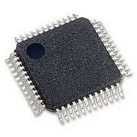
OX16C950-TQBG OXFORD SEMICONDUCTOR, OX16C950-TQBG Datasheet - Page 24

OX16C950-TQBG
Manufacturer Part Number
OX16C950-TQBG
Description
IC, UART, 1CH, SMD, TQFP48, 950
Manufacturer
OXFORD SEMICONDUCTOR
Datasheet
1.OX16C950-TQBG.pdf
(50 pages)
Specifications of OX16C950-TQBG
No. Of Channels
1
Data Rate
15Mbps
Uart Features
Tx/Rx FIFO INT TRIG
Supply Voltage Range
3V To 5.25V
Operating Temperature Range
0°C To +70°C
Digital Ic Case Style
TQFP
No. Of Pins
48
Lead Free Status / RoHS Status
Lead free / RoHS Compliant
Available stocks
Company
Part Number
Manufacturer
Quantity
Price
Company:
Part Number:
OX16C950-TQBG
Manufacturer:
SAMSUNG
Quantity:
450
LSR[6]: Transmitter and THR empty
logic 0 ⇒ The transmitter is not idle
logic 1 ⇒ THR is empty and the transmitter has
LSR[7]: Receiver data error
logic 0 ⇒ Either there are no receiver data errors in the
logic 1 ⇒ At least one parity error, framing error or break
In 450 mode LSR[7] is permanently cleared, otherwise this
bit will be set when an erroneous character is transferred
from the receiver to the RHR. It is cleared when the LSR is
read. Note that in 16C550 this bit is only cleared when
all of the erroneous data are removed from the FIFO. In
9-bit data framing mode parity is permanently disabled, so
this bit is not affected by LSR[2].
10
The serial channel interrupts are asserted on the INT pin.
When INTSEL# is high or unconnected, the INT pin is
forcing logic and MCR[3] is ignored. When INTSEL# is low,
the tri-state control of INT is controlled by MCR[3]. In this
case the INT pin is forcing when MCR[3] is set. It is in high-
impedance state when MCR[3] is cleared.
10.1
Serial channel interrupts are enabled using the Interrupt
Enable Register (‘IER’).
IER[0]: Receiver data available interrupt mask
logic 0 ⇒ Disable the receiver ready interrupt.
logic 1 ⇒Enable the receiver ready interrupt.
IER[1]: Transmitter empty interrupt mask
logic 0 ⇒Disable the transmitter empty interrupt.
logic 1 ⇒Enable the transmitter empty interrupt.
IER[2]: Receiver status interrupt
Normal mode:
logic 0 ⇒ Disable the receiver status interrupt.
logic 1 ⇒ Enable the receiver status interrupt.
9-bit data mode:
logic 0 ⇒ Disable receiver status and address bit
logic 1 ⇒ Enable receiver status and address bit
DS-0031 Sep 05
OXFORD SEMICONDUCTOR LTD.
I
NTERRUPTS
Interrupt Enable Register ‘IER’
completed the character in shift register and is
in idle mode. (I.e. set whenever the transmitter
shift register and the THR are both empty.)
FIFO or it was cleared by an earlier read of
LSR.
indication in the FIFO.
interrupt.
interrupt.
& S
LEEP
M
ODE
External—Free Release
In 9-bit mode (i.e. when NMR[0] is set) reception of a
character with the address-bit (9
level 1 interrupt if IER[2] is set.
IER[3]: Modem status interrupt mask
logic 0 ⇒ Disable the modem status interrupt.
logic 1 ⇒ Enable the modem status interrupt.
IER[4]: Sleep mode
logic 0 ⇒ Disable sleep mode.
logic 1 ⇒ Enable sleep mode whereby the internal clock
Sleep mode is described in section 10.4.
IER[5]: Special character interrupt mask or alternate
sleep mode
9-bit data framing mode:
logic 0 ⇒ Disable the special character receive interrupt.
logic 1 ⇒ Enable the special character receive interrupt.
In 9-bit data mode, The receiver can detect up to four
special characters programmed in Special Character 1 to
4. When IER[5] is set, a level 5 interrupt is asserted when a
match is detected.
650/950 modes (non-9-bit data framing):
logic 0 ⇒ Disable the special character receive interrupt.
logic 1 ⇒ Enable the special character receive interrupt.
In 16C650 compatible mode when the device is in
Enhanced mode (EFR[4]=1), this bit enables the detection
of special characters. It enables both the detection of
XOFF characters (when in-band flow control is enabled via
EFR[3:0]) and the detection of the XOFF2 special
character (when enabled via EFR[5]).
750 mode (non-9-bit data framing):
logic 0 ⇒ Disable alternate sleep mode.
logic 1 ⇒ Enable alternate sleep mode whereby the
In 16C750 compatible mode (i.e. non-Enhanced mode),
this bit is used an alternate sleep mode and has the same
effect as IER[4]. (See section 10.4)
of the channel is switched off.
internal clock of the channel is switched off.
th
bit) set can generate a
OX16C950 rev B
Page 24


