EVAL-ADAU1761Z Analog Devices Inc, EVAL-ADAU1761Z Datasheet - Page 44
EVAL-ADAU1761Z
Manufacturer Part Number
EVAL-ADAU1761Z
Description
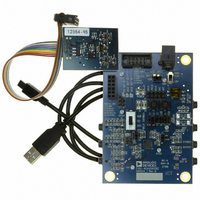
Eval Board For ADAU1761
Manufacturer
Analog Devices Inc
Series
SigmaDSP®r
Specifications of EVAL-ADAU1761Z
Main Purpose
Audio, CODEC
Embedded
Yes, DSP
Utilized Ic / Part
ADAU1761
Primary Attributes
Stereo, 24-Bit, 8 ~ 96 kHz Sampling Rate, GUI Tool
Secondary Attributes
I²C and GPIO Interfaces, 2 Differential and 1 Stereo Single-Ended Analog Inputs and Outputs
Silicon Manufacturer
Analog Devices
Core Architecture
SigmaDSP
Silicon Core Number
ADAU1761
Silicon Family Name
SigmaDSP
Application Sub Type
Audio
Lead Free Status / RoHS Status
Lead free / RoHS Compliant
Available stocks
Company
Part Number
Manufacturer
Quantity
Price
Company:

Part Number:
EVAL-ADAU1761Z
Manufacturer:
Analog Devices Inc
Quantity:
135


ADAU1761
APPLICATIONS INFORMATION
POWER SUPPLY BYPASS CAPACITORS
Each analog and digital power supply pin should be bypassed to
its nearest appropriate ground pin with a single 100 nF capaci-
tor. The connections to each side of the capacitor should be as
short as possible, and the trace should stay on a single layer with
no vias. For maximum effectiveness, locate the capacitor equi-
distant from the power and ground pins or, when equidistant
placement is not possible, slightly closer to the power pin.
Thermal connections to the ground planes should be made
on the far side of the capacitor.
Each supply signal on the board should also be bypassed with a
single bulk capacitor (10 μF to 47 μF).
GSM NOISE FILTER
In mobile phone applications, excessive 217 Hz GSM noise on
the analog supply pins can degrade the audio quality. To avoid
this problem, it is recommended that an L-C filter be used in
series with the bypass capacitors for the AVDD pins. This filter
should consist of a 1.2 nH inductor and a 9.1 pF capacitor in
series between AVDD and ground, as shown in Figure 64.
Figure 63. Recommended Power Supply Bypass Capacitor Layout
Figure 64. GSM Filter on the Analog Supply Pins
AVDD
CAPACITOR
TO VDD
AVDD
1.2nH
VDD
0.1µF
0.1µF
10µF
+
TO GND
9.1pF
GND
Rev. C | Page 44 of 92
GROUNDING
A single ground plane should be used in the application layout.
Components in an analog signal path should be placed away
from digital signals.
EXPOSED PAD PCB DESIGN
The ADAU1761 has an exposed pad on the underside of the
LFCSP. This pad is used to couple the package to the PCB for
heat dissipation when using the outputs to drive earpiece or
headphone loads. When designing a board for the ADAU1761,
special consideration should be given to the following:
•
•
A copper layer equal in size to the exposed pad should be
on all layers of the board, from top to bottom, and should
connect somewhere to a dedicated copper board layer (see
Figure 65).
Vias should be placed to connect all layers of copper,
allowing for efficient heat and energy conductivity. For an
example, see Figure 66, which has nine vias arranged in a
3 inch × 3 inch grid in the pad area.
Figure 65. Exposed Pad Layout Example, Side View
Figure 66. Exposed Pad Layout Example, Top View
VIAS
COPPER SQUARES
TOP
GROUND
POWER
BOTTOM
Related parts for EVAL-ADAU1761Z
Image
Part Number
Description
Manufacturer
Datasheet
Request
R


Part Number:
Description:
BOARD EVAL FOR SI270X-A
Manufacturer:
Silicon Laboratories Inc
Datasheet:

Part Number:
Description:
BUCK CONV REF DESIGN KIT IP1201
Manufacturer:
International Rectifier
Datasheet:
Part Number:
Description:
BOARD DEMO SYNC DUAL BUCK CNVTER
Manufacturer:
International Rectifier
Datasheet:
Part Number:
Description:
BOARD DEMO SYNC BUCK CONVETER
Manufacturer:
International Rectifier
Datasheet:

Part Number:
Description:
EVALBOARD/EB Omnidirectional microphone - Analog
Manufacturer:
Analog Devices
Datasheet:
Part Number:
Description:
EVALBOARD/EB Omnidirectional microphone - Analog
Manufacturer:
Analog Devices
Datasheet:


Part Number:
Description:
BOARD EVAL LED DRIVER LT3756
Manufacturer:
Linear Technology
Datasheet:

Part Number:
Description:
BOARD EVAL FOR AD7741/7742
Manufacturer:
Analog Devices Inc
Datasheet:

Part Number:
Description:
±1.7g Dual-Axis IMEMS Accelerometer Evaluation Board
Manufacturer:
Analog Devices Inc
Datasheet:

Part Number:
Description:
IC MULTIPLIER ANALOG 8-SOIC T/R
Manufacturer:
Analog Devices Inc
Datasheet:

Part Number:
Description:
IC ANALOG MULTIPLIER 8-DIP
Manufacturer:
Analog Devices Inc
Datasheet:
Part Number:
Description:
IC ANALOG MULTIPLIER 8-SOIC
Manufacturer:
Analog Devices Inc
Datasheet:
Part Number:
Description:
IC ANALOG MULTIPLIER 8-DIP
Manufacturer:
Analog Devices Inc
Datasheet: