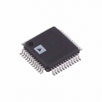
AD9874ABSTRL Analog Devices Inc, AD9874ABSTRL Datasheet - Page 13

AD9874ABSTRL
Manufacturer Part Number
AD9874ABSTRL
Description
IC,RF/Baseband Circuit,BICMOS,QFP,48PIN,PLASTIC
Manufacturer
Analog Devices Inc
Datasheet
1.AD9874-EB.pdf
(40 pages)
Specifications of AD9874ABSTRL
Rohs Status
RoHS non-compliant
Function
IF Digitizing Subsystem
Frequency
10MHz ~ 300MHz
Rf Type
UHF, Cellular, TETRA, GSM, EDGE, APCO25
Secondary Attributes
16dB Front End Attenuator
Package / Case
48-LQFP
For Use With
AD9874-EB - BOARD EVAL FOR AD9874
Lead Free Status / Rohs Status
Compliant
SERIAL PERIPHERAL INTERFACE (SPI)
The serial peripheral interface (SPI) is a bidirectional serial port. It is used to load configuration information into the registers listed
below as well as to read back their contents. Table I provides a list of the registers that may be programmed through the SPI port.
Addresses and default values are given in hexadecimal form.
Address Bit
(Hex)
POWER CONTROL REGISTERS
0x00
0x01
0x02
AGC
0x03
0x04
0x05
0x06
DECIMATION FACTOR
0x07
LO SYNTHESIZER
0x08
0x09
0x0A
0x0B
0x0C
0x0D
0x0E
REV. A
Breakdown Width
(7:0)
(7:6)
(5:4)
(3:2)
(1:0)
(7:0)
(7)
(6:0)
(7:0)
(7:4)
(3:0)
(7)
(6:4)
(3)
(2:0)
(7:5)
(4)
(3:0)
(5:0)
(7:0)
(7:5)
(4:0)
(7:0)
(6)
(5)
(4:2)
(1:0)
(5:0)
(7:0)
8
2
2
2
2
8
1
7
8
4
4
1
3
1
3
3
1
4
6
8
3
5
8
1
1
3
2
4
8
Default Value Name
0xFF
0
0
0
0
0x00
0
0x00
0x00
0
0
0
0
0
0
0
4
0x00
0x38
0x5
0x00
0x1D
0
0
0
3
0x0
0x04
STBY
LNAB
MIXB
ADCB
TEST
ATTEN
AGCG(14:8) AGC Attenuation Setting (7 MSB of a 15-Bit Unsigned Word).
AGCG(7:0) AGC Attenuation Setting (8 LSB of a 15-Bit Unsigned Word).
AGCA
AGCD
AGCV
AGCO
AGCF
AGCR
Unused
K
M
LOR(13:8)
LOR(7:0)
LOA
LOB(12:8)
LOB(7:0)
LOF
LOINV
LOI
LOTM
LOFA(13:8) LO Fast Acquire Time Unit (6 MSB of a 14-Bit Word).
LOFA(7:0)
CKOB
Table I. SPI Address Map
Description
Standby Control Bits (REF, LO, CKO, CK, GC, LNAMX, Unused,
and ADC).
LNA Bias Current (0 = 0.5 mA, 1 = 1 mA, 2 = 2 mA, 3 = 3 mA).
Mixer Bias Current (0 = 0.5 mA, 1 = 1.5 mA, 2 = 2.7 mA, 3 = 4 mA).
CK Oscillator Bias (0 = 0.25 mA, 1 = 0.35 mA, 2 = 0.40 mA, 3 = 0.65 mA).
Do not use.
Factory Test Mode. Do not use.
Apply 16 dB attenuation in the front end.
Default corresponds to maximum gain.
AGC Attack Bandwidth Setting. Default yields 50 Hz raw loop bandwidth.
AGC Decay Time Setting. Default is decay time = attack time.
Enable digital VGA to increase AGC range by 12 dB.
AGC Overload Update Setting. Default is slowest update.
Fast AGC (Minimizes resistance seen between GCP and GCN).
AGC Enable/Reference Level (Disabled, 3 dB, 6 dB, 9 dB, 12 dB, 15 dB
below Clip).
Decimation Factor = 60
Default is Decimate-by-300.
Reference Frequency Divisor (6 MSB of a 14-Bit Word).
Reference Frequency Divisor (8 LSB of a 14-Bit Word).
Default (56) yields 300 kHz from f
“A” Counter (Prescaler Control Counter).
“B” Counter MSB (5 MSB of a 13-Bit Word).
Default LOA and LOB values yield 300 kHz from 73.35 MHz to 2.25 MHz.
“B” Counter LSB (8 LSB of a 13-Bit Word).
Enable fast acquire.
Invert charge pump (0 = source current to increase VCO frequency).
Charge Pump Current in Normal Operation. I
Manual Control of LO Charge Pump (0 = Off, 1 = Up, 2 = Down,
3 = Normal).
LO Fast Acquire Time Unit (8 LSB of a 14-Bit Word).
–13–
(M + 1), if K = 0; 48
REF
= 16.8 MHz.
PUMP
= (LOI + 1)
(M + 1), if K = 1.
AD9874
0.625 mA.


