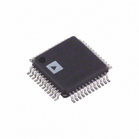
AD9874ABSTRL Analog Devices Inc, AD9874ABSTRL Datasheet - Page 22

AD9874ABSTRL
Manufacturer Part Number
AD9874ABSTRL
Description
IC,RF/Baseband Circuit,BICMOS,QFP,48PIN,PLASTIC
Manufacturer
Analog Devices Inc
Datasheet
1.AD9874-EB.pdf
(40 pages)
Specifications of AD9874ABSTRL
Rohs Status
RoHS non-compliant
Function
IF Digitizing Subsystem
Frequency
10MHz ~ 300MHz
Rf Type
UHF, Cellular, TETRA, GSM, EDGE, APCO25
Secondary Attributes
16dB Front End Attenuator
Package / Case
48-LQFP
For Use With
AD9874-EB - BOARD EVAL FOR AD9874
Lead Free Status / Rohs Status
Compliant
AD9874
Figure 7c. CLK Phase Noise vs. Charge Pump Setting Bias
(IF = 73.35 MHz, IF = 71.1 MHz, –31 dBm, f
f
and CKN = 60 with f
Address Bit
(Hex)
0x00
0x01
0x10
0x11
0x12
0x13
0x14
0x15
0x16
IF LNA/MIXER
The AD9874 contains a single-ended LNA followed by a Gil-
bert-type active mixer, shown in Figure 8 with the required
external components. The LNA uses negative shunt feedback to
set its input impedance at the IFIN pin, thus making it depen-
dent on the LNA bias setting and input frequency. It can be
modeled as approximately 370 Ω//1.4 pF (620%) for the higher
bias settings below 100 MHz. Figures 9a and 9b show the
equivalent input impedance versus frequency characteristics of
the AD9874 with all the LNA bias settings. The increase in shunt
resistance versus frequency can be attributed to the reduction in
bandwidth, thus the amount of negative feedback of the LNA.
Note that the input signal into IFIN should be ac-coupled via a
10 nF capacitor since the LNA input is self-biasing.
REF
Table VIII. SPI Registers Associated with CLK Synthesizer
= 16.8 MHz) (CLK SYN Settings: CKO Bias = 3, CKR = 56,
–100
–110
–120
–130
–140
–10
–20
–30
–40
–50
–60
–70
–80
–90
0
–25
Breakdown Width
(7:0)
(3:2)
(5:0)
(7:0)
(4:0)
(7:0)
(6)
(5)
(4:2)
(1:0)
(3:0)
(7:0)
–20
–15
REF
CP = 2
–10
CP = 0
FREQUENCY OFFSET – kHz
= 300 kHz)
8
2
6
8
5
8
1
1
3
1
4
8
–5
0
Default
Value
0xFF
0
00
0x38
0x00
0x3C
0
0
0
0
0x0
0x04
5
CP = 4
CP = 6
EXT CLK
10
CLK
15
= 18 MHz,
Name
STBY
CKOB
CKR(13:8)
CKR(7:0)
CKN(12:8)
CKN(7:0)
CKF
CKINV
CKI
CKTM
CKFA(13:8)
CKFA(7:0)
20
25
–22–
IFIN
Figure 8. Simplified Schematic of AD9874’s LNA/Mixer
R
Figure 9a. The Shunt Input Resistance vs. the
Frequency of the AD9874’s IF1 Input
Figure 9b. The Shunt Capacitance vs.
the Frequency of the AD9874’s IF1 Input
VDDI
F
2.5
2.0
1.5
1.0
0.5
600
550
500
450
400
350
300
0
R
R
0
BIAS
GAIN
0
LNA BIAS = 1
50
50
CXVL
MXOP
100
100
L
LNA BIAS = 0
FREQUENCY – MHz
FREQUENCY – MHz
MULTI-TANH
V–I STAGE
150
2.7V TO 3.6V
150
LNA BIAS = 0
LNA BIAS = 2
C
50
LNA BIAS = 1
200
200
LNA BIAS = 3
M X ON
L
250
250
DC SERVO
LOOP
LNA BIAS = 3
LNA BIAS = 2
300
300
CXIF
LO INPUT =
0.3V p-p TO
1.0V p-p
CXVM
REV. A
350
350


