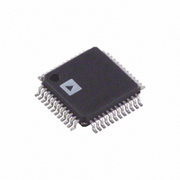
AD9874ABSTRL Analog Devices Inc, AD9874ABSTRL Datasheet - Page 28

AD9874ABSTRL
Manufacturer Part Number
AD9874ABSTRL
Description
IC,RF/Baseband Circuit,BICMOS,QFP,48PIN,PLASTIC
Manufacturer
Analog Devices Inc
Datasheet
1.AD9874-EB.pdf
(40 pages)
Specifications of AD9874ABSTRL
Rohs Status
RoHS non-compliant
Function
IF Digitizing Subsystem
Frequency
10MHz ~ 300MHz
Rf Type
UHF, Cellular, TETRA, GSM, EDGE, APCO25
Secondary Attributes
16dB Front End Attenuator
Package / Case
48-LQFP
For Use With
AD9874-EB - BOARD EVAL FOR AD9874
Lead Free Status / Rohs Status
Compliant
AD9874
VARIABLE GAIN AMPLIFIER OPERATION WITH
AUTOMATIC GAIN CONTROL
The AD9874 contains both a variable gain amplifier (VGA) and
a digital VGA (DVGA) along with all of the necessary signal
estimation and control circuitry required to implement auto-
matic gain control (AGC), as shown in Figure 18. The AGC
control circuitry provides a high degree of programmability,
allowing users to optimize the AGC response as well as the
AD9874’s dynamic range for a given application. The VGA is
programmable over a 12 dB range and implemented within the
ADC by adjusting its full-scale reference level. Increasing the
ADC’s full scale is equivalent to attenuating the signal. An
additional 12 dB of digital gain range is achieved by scaling the
output of the decimation filter in the DVGA. Note that a slight
increase in the supply current (i.e., 0.67 mA) is drawn from
VDDI and VDDF as the VGA changes from 0 dB to 12 dB
attenuation.
The purpose of the VGA is to extend the usable dynamic range
of the AD9874 by allowing the ADC to digitize a desired signal
over a large input power range as well as recover a low level
signal in the presence of larger unfiltered interferers without
saturating or clipping the ADC. The DVGA is most useful in
extending the dynamic range in narrow-band applications
requiring a 16-bit I and Q data format. In these applications,
quantization noise resulting from internal truncation to 16 bits
as well as external 16-bit fixed point post-processing can
degrade the AD9874’s effective noise figure by 1 dB or more.
The DVGA is enabled by writing a 1 to the AGCV field. The
VGA (and the DVGA) can operate in either a user controlled
Variable Gain Mode or Automatic Gain Control (AGC) Mode.
It is worth noting that the VGA imparts negligible phase error
upon the desired signal as its gain is varied over a 12 dB range.
This is due to the bandwidth of the VGA being far greater than
the downconverted desired signal (centered about f
remaining relatively independent of gain setting. As a result,
phase modulated signals should experience minimal phase error
as the AGC varies the VGA gain while tracking an interferer or
the desired signal under fading conditions. Note that the enve-
lope of the signal will still be affected by the AGC settings.
GCP
- ADC
FS
C
DAC
DEC1
VGA
DAC
12
Figure 18. Functional Block Diagram of VGA and AGC
DEC2
DEC3
AND
I + Q
I + Q
CLK
/8) and
LARGER
SELECT
–28–
REF LEVEL
AGCR
+
AGCA/AGCD
Variable Gain Control
The variable gain control is enabled by setting the AGCR field
of Register 0x06 to 0. In this mode, the gain of the VGA (and
the DVGA) can be adjusted by writing to the 16-bit AGCG
register. The maximum update rate of the AGCG register via
the SPI port is f
enables 16 dB of attenuation in the mixer. This feature allows
the AD9874 to cope with large level signals beyond the VGA’s
range (i.e., > –18 dBm at LNA input) to prevent overloading
of the ADC.
The lower 15 bits specify the attenuation in the remainder of
the signal path. If the DVGA is enabled, the attenuation range
is from –12 dB to +12 dB since the DVGA provides 12 dB of
digital gain. In this case, all 15 bits are significant. However,
with the DVGA disabled, the attenuation range extends from
0 dB to 12 dB and only the lower 14 bits are useful. Figure 19
shows the relationship between the amount of attenuation and
the AGC register setting for both cases.
SCALING
K
–12
Figure 19. AGC Gain Range Characteristics vs.
AGCG Register Setting with and without DVGA
Enabled
12
–6
0000
6
0
(1 – Z
VGA ENABLED
1
RSSI DATA
–1
ONLY
)
CLK
SETTING
AGCV
VGA ENABLED
1FFF
/240. The MSB of this register is the bit that
DVGA AND
AGCG SETTING – HEX
3FFF
DVGA
I/Q DATA
TO SSI
TO SSI
5FFF
7FFF
RANGE
RANGE
REV. A
DVGA
VGA


