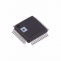
AD9874ABSTRL Analog Devices Inc, AD9874ABSTRL Datasheet - Page 36

AD9874ABSTRL
Manufacturer Part Number
AD9874ABSTRL
Description
IC,RF/Baseband Circuit,BICMOS,QFP,48PIN,PLASTIC
Manufacturer
Analog Devices Inc
Datasheet
1.AD9874-EB.pdf
(40 pages)
Specifications of AD9874ABSTRL
Rohs Status
RoHS non-compliant
Function
IF Digitizing Subsystem
Frequency
10MHz ~ 300MHz
Rf Type
UHF, Cellular, TETRA, GSM, EDGE, APCO25
Secondary Attributes
16dB Front End Attenuator
Package / Case
48-LQFP
For Use With
AD9874-EB - BOARD EVAL FOR AD9874
Lead Free Status / Rohs Status
Compliant
AD9874
and digital driver strength should be set to their lowest pos-
sible settings to minimize the potential harmful effects of
digital induced noise while preserving a reliable data link to
the DSP. Note that the SSICRA, SSICRB, and SSIORD
registers (i.e., 0x18, 0x19, and 0x1A) provide a large degree
of flexibility for optimization of the SSI interface.
Synchronization of Multiple AD9874s
Some applications such as receiver diversity and beam steering
may require two or more AD9874s operating in parallel while
maintaining synchronization. Figure 28 shows an example of
how multiple AD9874s can be cascaded, with one device serv-
ing as the master and the other devices serving as the slaves. In
this example, all of the devices have the same SPI register con-
figuration since they share the same SPI interface to the DSP.
Since the state of each of the AD9874’s internal counters is
unknown upon initialization, synchronization of the devices is
required via a SYNCB pulse (see Figure 4) to synchronize their
digital filters and ensure precise time alignment of the data
streams.
Although all of the devices’ synthesizers are enabled, the LO
and CLK signals for the slaves(s) are derived from the masters’
synthesizers and are referenced to an external crystal oscillator.
All of the necessary external components (i.e., loop filters,
varactor, LC, and VCO) required to ensure proper closed-loop
operation of these synthesizers are included.
Note that although the VCO output of the LO synthesizer is
ac-coupled to the slave’s LO input(s), all of the CLK inputs of
the devices must be dc-coupled if the AD9874’s CLK oscillators
are enabled. This is due to the dc current required by the CLK
oscillators in each device. In essence, these negative impedance
cores are operating in parallel, increasing the effective Q of the
LC resonator circuit. Note that RBIAS should be sized such
that the sum of the oscillators’ dc bias currents maintains a
common-mode voltage of around 1.6 V.
–36–
0.1 F
Figure 28. Example of Synchronizing Multiple AD9874s
TO OTHER
AD9874s
R
VDDC
L
BIAS
OSC
C
VCO
OSC
C
R
VAR
D
47
43
42
19
20
47
42
19
20
43
FILTER
IFIN
LOP
LON
CLKP
CLKN
LOOP
CLKP
CLKN
IFIN
LOP
LON
C
C
P
Z
R
F
IOUTL
IOUTC
IOUTC
AD9874
AD9874
MASTER
15
38
FILTER
15
SLAVE
LOOP
CLKOUT
CLKOUT
SYNCB
SYNCB
DOUTA
DOUTA
f
f
REF
REF
PD
PC
PD
PC
FS
PE
PE
FS
25
24
23
33
31
29
35
35
31
29
28
25
24
23
33
28
TO OTHER
AD9874s
FROM
CRYSTAL
OSCILLATION
TO
DSP
TO DSP
REV. A
FROM
DSP


