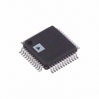
AD9874ABSTRL Analog Devices Inc, AD9874ABSTRL Datasheet - Page 6

AD9874ABSTRL
Manufacturer Part Number
AD9874ABSTRL
Description
IC,RF/Baseband Circuit,BICMOS,QFP,48PIN,PLASTIC
Manufacturer
Analog Devices Inc
Datasheet
1.AD9874-EB.pdf
(40 pages)
Specifications of AD9874ABSTRL
Rohs Status
RoHS non-compliant
Function
IF Digitizing Subsystem
Frequency
10MHz ~ 300MHz
Rf Type
UHF, Cellular, TETRA, GSM, EDGE, APCO25
Secondary Attributes
16dB Front End Attenuator
Package / Case
48-LQFP
For Use With
AD9874-EB - BOARD EVAL FOR AD9874
Lead Free Status / Rohs Status
Compliant
AD9874
Pin
1
2
3
4
5
6
7
8
9
10
11
12
13
14
15
16
17
18
19
20
21
22
23
24
25
26
Mnemonic
MXOP
MXON
GNDF
IF2N
IF2P
VDDF
GCP
GCN
VDDA
GNDA
VREFP
VREFN
RREF
VDDQ
IOUTC
GNDQ
VDDC
GNDC
CLKP
CLKN
GNDS
GNDD
PC
PD
PE
VDDD
Description
Mixer Output, Positive.
Mixer Output, Negative.
Ground for Front End of ADC.
Second IF Input (to ADC), Negative.
Second IF Input (to ADC), Positive.
Positive Power Supply for Front End of ADC.
Filter Capacitor for ADC Full-Scale Control.
Full-Scale Control Ground.
Positive Power Supply for ADC Back End.
Ground for ADC Back End.
Voltage Reference, Positive.
Voltage Reference, Negative.
Reference Resistor: Requires 100 kΩ to
GNDA.
Positive Power Supply for Clock Synthesizer.
Clock Synthesizer Charge Pump Output
Current.
Ground for Clock Synthesizer Charge
Pump.
Positive Power Supply for Clock Synthesizer.
Ground for Clock Synthesizer.
Sampling Clock Input/Clock VCO Tank,
Positive.
Sampling Clock Input/Clock VCO Tank,
Negative.
Substrate Ground.
Ground for Digital Functions.
Clock Input for SPI Port.
Data I/O for SPI Port.
Enable Input for SPI Port.
Positive Power Supply for Internal Digital
Function.
VREFP
VREFN
MXON
MXOP
GNDA
GNDF
VDDA
VDDF
GCN
IF2N
IF2P
GCP
PIN FUNCTION DESCRIPTIONS
10
11
12
1
2
3
4
5
6
7
8
9
13
48 47 46 45 44
PIN 1
IDENTIFIER
PIN CONFIGURATION
14
15
16
(Not to Scale)
17
AD9874
TOP VIEW
18
43
–6–
19
42
41
20 21 22 23 24
Pin
27
28
29
30
31
32
33
34
35
36
37
38
39
40
41
42
43
44
45
46
47
48
40
39 38 37
Mnemonic
VDDH
CLKOUT
DOUTA
DOUTB
FS
GNDH
SYNCB
GNDS
FREF
GNDL
GNDP
IOUTL
VDDP
VDDL
CXVM
LON
LOP
CXVL
GNDI
CXIF
IFIN
VDDI
36
35
34
33
32
31
30
29
28
26
25
27
GNDL
FREF
GNDS
SYNCB
GNDH
FS
DOUTB
DOUTA
CLKOUT
VDDH
VDDD
PE
Clock Output for SSI Port.
Data Output for SSI Port.
Data Output for SSI Port (Inverted) or
Ground for Digital Interface.
Resets SSI and Decimator Counters;
Substrate Ground.
Reference Frequency Input for Both
Ground for LO Synthesizer.
Ground for LO Synthesizer Charge Pump.
LO Synthesizer Charge Pump Output
Positive Power Supply for LO Synthesizer
Positive Power Supply for LO Synthesizer.
External Filter Capacitor; DC Output of
External Bypass Capacitor for LNA Power
Ground for Mixer and LNA.
External Capacitor for Mixer V-I Con-
First IF Input (to LNA).
Positive Power Supply for LNA and Mixer.
Description
Positive Power Supply for Digital Interface.
SPI Port.
Frame Sync for SSI Port.
Active Low.
Synthesizers.
Current Charge Pump.
Charge Pump.
LNA.
LO Input to Mixer and LO Synthesizer,
Negative.
LO Input to Mixer and LO Synthesizer,
Positive.
Supply.
verter Bias.
REV. A


