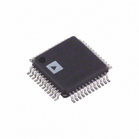
AD9874ABSTRL Analog Devices Inc, AD9874ABSTRL Datasheet - Page 25

AD9874ABSTRL
Manufacturer Part Number
AD9874ABSTRL
Description
IC,RF/Baseband Circuit,BICMOS,QFP,48PIN,PLASTIC
Manufacturer
Analog Devices Inc
Datasheet
1.AD9874-EB.pdf
(40 pages)
Specifications of AD9874ABSTRL
Rohs Status
RoHS non-compliant
Function
IF Digitizing Subsystem
Frequency
10MHz ~ 300MHz
Rf Type
UHF, Cellular, TETRA, GSM, EDGE, APCO25
Secondary Attributes
16dB Front End Attenuator
Package / Case
48-LQFP
For Use With
AD9874-EB - BOARD EVAL FOR AD9874
Lead Free Status / Rohs Status
Compliant
The signal transfer function of the AD9874 possesses inherent
antialias filtering by virtue of the continuous-time portions of
the loop filter in the band-pass - modulator. Figure 13b
illustrates this property by plotting the nominal signal transfer
function of the ADC for frequencies up to 2f
that naturally occur for all frequencies that alias to the f
pass band are clearly visible. Even at the widest bandwidth setting,
the notches are deep enough to provide greater than 80 dB of
alias protection. Thus, the wideband IF filtering requirements
preceding the AD9874 will be determined mostly by the mixer’s
image band, which is offset from the desired IF input frequency
by f
with the ADC.
Figure 13c shows the nominal signal transfer function magni-
tude for frequencies near the f
pass band determines the transfer function droop, but even at
the lowest oversampling ratio (48) where the pass band edges
are at
0.5 dB. Note that the amount of attenuation offered by the
signal transfer function near f
when determining the narrow-band IF filtering requirements
preceding the AD9874.
REV. A
CLK
/4 (i.e., 2 3 f
–10
–15
–20
–10
–20
–30
–40
–50
–60
–70
–80
Figure 13b. Signal Transfer Function of the
Band-Pass - Modulator from 0 f
–5
f
0
0
CLK
–0.10
Figure 13c. Magnitude of the ADC’s Signal
Transfer Function near f
0
/192 (
NORMALIZED FREQUENCY – RELATIVE TO
NORMALIZED FREQUENCY – RELATIVE TO
CLK
–0.05
0.005 f
0.5
/8) rather than any aliasing associated
NOTCH AT ALL ALIAS FREQUENCIES
CLK
CLK
CLK
), the gain variation is less than
/8 should also be considered
1.0
/8 pass band. The width of the
0
CLK
/8
0.05
CLK
1.5
CLK
. The notches
f
f
CLK
OUT
to 2 f
CLK
CLK
0.10
2.0
/8
–25–
Tuning of the - modulator’s two continuous-time resonators
is essential in realizing the ADC’s full dynamic range and must
be performed upon system startup. To facilitate tuning of the
LC tank, a capacitor array is internally connected to the MXOP
and MXON pins. The capacitance of this array is program-
mable from 0 pF to 200 pF
either automatically or manually via the SPI port. The capaci-
tors of the active RC resonator are similarly programmable.
Note that the AD9874 can be placed in and out of its standby
mode without retuning since the tuning codes are stored in the
SPI Registers.
When tuning the LC tank, the sampling clock frequency must
be stable and the LNA/mixer, LO synthesizer, and ADC must
all be placed in standby. Tuning is triggered when the ADC is
taken out of standby if the TUNE_LC bit of Register 0x1C has
been set. This bit will clear when the tuning operation is com-
plete (less than 6 ms). The tuning codes can be read from the
3-bit CAPL1 (0x1D) and the 6-bit CAPL0 (0x1E) registers.
In a similar manner, tuning of the RC resonator is activated if
the TUNE_RC bit of Register 0x1C is set when the ADC is
taken out of standby. This bit will clear when tuning is com-
plete. The tuning code can be read from the CAPR (0x1F)
register. Setting both the TUNE_LC and TUNE_RC bits tunes
the LC tank and the active RC resonator in succession. During
tuning, the ADC is not operational and neither data nor a clock
is available from the SSI port. Table X lists the recommended
sequence of the SPI commands for tuning the ADC, and Table XI
lists all of the SPI registers associated with band-pass - ADC.
Address Value Comments
0x00
0x1C
0x00
*If external CLK VCO or source used, the CLK oscillator must also be disabled.
Address Bit
(Hex)
0x00
0x1C
0x1D
0x1E
0x1F
Table XI. SPI Registers Associated with Band-Pass - ADC
0x45
0x03
0x44
Breakdown
(7:0)
(1)
(0)
(2:0)
(5:0)
(7:0)
Table X. Tuning Sequence
LO synthesizer, LNA/mixer, and ADC are
placed in standby.*
Set TUNE_LC and TUNE_RC. Wait for
CLK to stabilize if CLK synthesizer used.
Take the ADC out of standby. Wait for
0x1C to clear (<6 ms). LNA/mixer can now
be taken out of standby.
Width
8
1
1
3
6
8
20% and can be programmed
0xFF
0
0
0
0x00
0x00
Default
Value
AD9874
Name
STBY
TUNE_LC
TUNE_RC
CAPL1(2:0)
CAPL1(5:0)
CAPR


