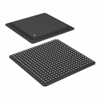
ADSP-21160NCB-100 Analog Devices Inc, ADSP-21160NCB-100 Datasheet - Page 14

ADSP-21160NCB-100
Manufacturer Part Number
ADSP-21160NCB-100
Description
IC,DSP,32-BIT,CMOS,BGA,400PIN,PLASTIC
Manufacturer
Analog Devices Inc
Series
SHARC®r
Type
Floating Pointr
Specifications of ADSP-21160NCB-100
Rohs Status
RoHS non-compliant
Interface
Host Interface, Link Port, Serial Port
Clock Rate
100MHz
Non-volatile Memory
External
On-chip Ram
512kB
Voltage - I/o
3.30V
Voltage - Core
1.90V
Operating Temperature
-40°C ~ 100°C
Mounting Type
Surface Mount
Package / Case
400-BGA
Package
400BGA
Numeric And Arithmetic Format
Floating-Point
Maximum Speed
100 MHz
Ram Size
512 KB
Device Million Instructions Per Second
100 MIPS
Lead Free Status / RoHS Status
Available stocks
Company
Part Number
Manufacturer
Quantity
Price
Company:
Part Number:
ADSP-21160NCB-100
Manufacturer:
Analog Devices Inc
Quantity:
10 000
ADSP-21160M/ADSP-21160N
Table 3. Pin Function Descriptions (Continued)
Table 4. Boot Mode Selection
Pin
CLKOUT
RESET
TCK
TMS
TDI
TDO
TRST
EMU
CIF
V
V
AV
AGND
GND
NC
EBOOT
1
0
0
0
0
1
DDINT
DDEXT
DD
LBOOT
0
0
1
0
1
1
Type
O/T
I/A
I
I/S
I/S
O
I/A
O (O/D)
O/T
P
P
P
G
G
BMS
Output
1 (Input)
1 (Input)
0 (Input)
0 (Input)
x (Input)
Function
Local Clock Out. CLKOUT is driven at the CLKIN frequency by the processor. This output can be
three-stated by setting the COD bit in the SYSCON register. A keeper latch on the DSP’s CLKOUT
pin maintains the output at the level it was last driven (only enabled on the processor with
ID2-0 = 00x). Do not use CLKOUT in multiprocessing systems; use CLKIN instead.
Processor Reset. Resets the ADSP-21160x to a known state and begins execution at the program
memory location specified by the hardware reset vector address. The RESET input must be asserted
(low) at power-up.
Test Clock (JTAG). Provides a clock for JTAG boundary scan.
Test Mode Select (JTAG). Used to control the test state machine. TMS has a 20 kΩ internal pull-up
resistor.
Test Data Input (JTAG). Provides serial data for the boundary scan logic. TDI has a 20 kΩ internal
pull-up resistor.
Test Data Output (JTAG). Serial scan output of the boundary scan path.
Test Reset (JTAG). Resets the test state machine. TRST must be asserted (pulsed low) after power-
up or held low for proper operation of the ADSP-21160x. TRST has a 20 kΩ internal pull-up resistor.
EMU has a 50 kΩ internal pull-up resistor.
Core Instruction Fetch. Signal is active low when an external instruction fetch is performed. Driven
by bus master only. Three-state when host is bus master. CIF has a 20 kΩ internal pull-up resistor
that is enabled on the ADSP-21160x with ID2–0 = 00x.
Core Power Supply. Nominally 2.5 V (ADSP-21160M) or 1.9 V (ADSP-21160N) dc and supplies the
DSP’s core processor
I/O Power Supply. Nominally 3.3 V dc.
Analog Power Supply. Nominally 2.5 V (ADSP-21160M) or 1.9 V (ADSP-21160N) dc and supplies the
DSP’s internal PLL (clock generator). This pin has the same specifications as V
filtering circuitry is required. For more information, see Power Supplies on page 8.
Analog Power Supply Return.
Power Supply Return.
Do Not Connect. Reserved pins that must be left open and unconnected.
Emulation Status. Must be connected to the ADSP-21160x emulator target board connector only.
Booting Mode
EPROM (Connect BMS to EPROM chip select.)
Host Processor
Link Port
No Booting. Processor executes from external memory.
Reserved
Reserved
Rev. B | Page 14 of 60 | February 2010
DDINT
, except that added


