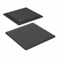
ADSP-21160NCB-100 Analog Devices Inc, ADSP-21160NCB-100 Datasheet - Page 47

ADSP-21160NCB-100
Manufacturer Part Number
ADSP-21160NCB-100
Description
IC,DSP,32-BIT,CMOS,BGA,400PIN,PLASTIC
Manufacturer
Analog Devices Inc
Series
SHARC®r
Type
Floating Pointr
Specifications of ADSP-21160NCB-100
Rohs Status
RoHS non-compliant
Interface
Host Interface, Link Port, Serial Port
Clock Rate
100MHz
Non-volatile Memory
External
On-chip Ram
512kB
Voltage - I/o
3.30V
Voltage - Core
1.90V
Operating Temperature
-40°C ~ 100°C
Mounting Type
Surface Mount
Package / Case
400-BGA
Package
400BGA
Numeric And Arithmetic Format
Floating-Point
Maximum Speed
100 MHz
Ram Size
512 KB
Device Million Instructions Per Second
100 MIPS
Lead Free Status / RoHS Status
Available stocks
Company
Part Number
Manufacturer
Quantity
Price
Company:
Part Number:
ADSP-21160NCB-100
Manufacturer:
Analog Devices Inc
Quantity:
10 000
OUTPUT DRIVE CURRENTS—ADSP-21160M
Figure 29
ers of the ADSP-21160M. The curves represent the current
drive capability of the output drivers as a function of output
voltage.
OUTPUT DRIVE CURRENTS—ADSP-21160N
Figure 30
ers of the ADSP-21160N. The curves represent the current drive
capability of the output drivers as a function of output voltage.
POWER DISSIPATION
Total power dissipation has two components: one due to inter-
nal circuitry and one due to the switching of external output
drivers.
–100
–120
120
100
–20
–40
–60
–80
–20
–40
–60
–80
80
60
40
20
80
60
40
20
0
0
shows typical I–V characteristics for the output driv-
shows typical I–V characteristics for the output driv-
0
0
Figure 29. ADSP-21160M Typical Drive Currents
V
Figure 30. ADSP-21160N Typical Drive Currents
V
DDEXT
DDEXT
0.5
0.5
V
= 3.47V, 0°C
= 3.11V, 115°C
DDEXT
V
DDEXT
V
OL
V
SOURCE (V
V
SWEEP (V
DDEXT
= 3.47V, –45°C
DDEXT
1
1
= 3.47V, 0°C
= 3.3V, 25°C
= 3.3V, 25°C
V
1.5
1.5
V
DDEXT
DDEXT
DDEXT
DDEXT
V
V
DDEXT
DDEXT
) VOLTAGE – V
) VOLTAGE – V
= 3.3V, 25°C
= 3.11V, 115°C
2
2
85°C
= 3.47V, –45°C
= 3.13V,
V
OH
V
DDEXT
V
DDEXT
2.5
2.5
85°C
= 3.13V,
= 3.3V, 25°C
Rev. B | Page 47 of 60 | February 2010
3
3
3.5
3.5
Internal power dissipation is dependent on the instruction
execution sequence and the data operands involved. Using the
current specifications (I
I
Page 16
Page 18
Table
internal power supply (V
application, according to the formula:
The external component of total power dissipation is caused by
the switching of output pins. Its magnitude depends on:
and is calculated by:
The load capacitance should include the processor’s package
capacitance (C
load high and then back low. Address and data pins can drive
high and low at a maximum rate of 1/(2t
can switch every cycle at a frequency of 1/t
at 1/(2t
Example for ADSP-21160N: Estimate P
assumptions:
The P
can drive, as shown in
conditions by adding a typical internal power dissipation:
where:
A typical power consumption can now be calculated for these
DD-IDLE
• The number of output pins that switch during each
• The maximum frequency at which they can switch (f)
• Their load capacitance (C)
• Their voltage swing (V
• A system with one bank of external data memory—
• Four 64K × 16 RAM chips are used, each with a load
• External data memory writes occur every other cycle, a rate
• The bus cycle time is 50 MHz (t
• P
• P
• P
+ % Peak × I
cycle (O)
asynchronous RAM (64-bit)
of 10 pF
of 1/(2 t
Power Dissipation on page
trical Characteristics—ADSP-21160M on Page 16
Electrical Characteristics—ADSP-21160N on Page 18
% Peak × I
% High × I
% Low × I
EXT
37, engineers can estimate the ADSP-21160x DSP’s
EXT
INT
PLL
) from
CK
and
and the current-versus-operation information in
equation is calculated for each class of pins that
is I
is AI
), but selects can switch on each cycle.
is from
P
DDINT
Electrical Characteristics—ADSP-21160N on
CK
TOTAL
= I
DD
Electrical Characteristics—ADSP-21160M on
P
IN
), with 50% of the pins switching
EXT
DD
DDINT
DD
DD
). The switching frequency includes driving the
DD
× 1.9 V, using the value for AI
ADSP-21160M/ADSP-21160N
Table 38
-
-
× 1.9 V, using the calculation I
-
INLOW
-
IDLE
= P
INPEAK
INHIGH
= O × C × V
EXT
Table
DD-INPEAK
DDINT
+ P
DD
INT
38.
)
) input current for a specific
DD
+ P
47
, I
2
DD-INHIGH
× f
PLL
CK
= 20 ns).
CK
EXT
CK
, I
). The write strobe
with the following
. Select pins switch
DD-INLOW
DD
DDINT
listed in
, and
listed in
and
Elec-


