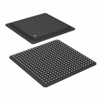
ADSP-21160NCB-100 Analog Devices Inc, ADSP-21160NCB-100 Datasheet - Page 6

ADSP-21160NCB-100
Manufacturer Part Number
ADSP-21160NCB-100
Description
IC,DSP,32-BIT,CMOS,BGA,400PIN,PLASTIC
Manufacturer
Analog Devices Inc
Series
SHARC®r
Type
Floating Pointr
Specifications of ADSP-21160NCB-100
Rohs Status
RoHS non-compliant
Interface
Host Interface, Link Port, Serial Port
Clock Rate
100MHz
Non-volatile Memory
External
On-chip Ram
512kB
Voltage - I/o
3.30V
Voltage - Core
1.90V
Operating Temperature
-40°C ~ 100°C
Mounting Type
Surface Mount
Package / Case
400-BGA
Package
400BGA
Numeric And Arithmetic Format
Floating-Point
Maximum Speed
100 MHz
Ram Size
512 KB
Device Million Instructions Per Second
100 MIPS
Lead Free Status / RoHS Status
Available stocks
Company
Part Number
Manufacturer
Quantity
Price
Company:
Part Number:
ADSP-21160NCB-100
Manufacturer:
Analog Devices Inc
Quantity:
10 000
ADSP-21160M/ADSP-21160N
Dual-Ported On-Chip Memory
The ADSP-21160x contains four megabits of on-chip SRAM,
organized as two blocks of 2M bits each, which can be config-
ured for different combinations of code and data storage
(Figure
independent accesses by the core processor and I/O processor.
The dual-ported memory in combination with three separate
on-chip buses allows two data transfers from the core and one
from I/O processor, in a single cycle. The ADSP-21160x mem-
ory can be configured as a maximum of 128K words of
32-bit data, 256K words of 16-bit data, 85K words of 48-bit
instructions (or 40-bit data), or combinations of different word
sizes up to four megabits. All of the memory can be accessed as
16-, 32-, 48-, or 64-bit words. A 16-bit floating-point storage
format is supported that effectively doubles the amount of data
that may be stored on-chip. Conversion between the 32-bit
floating-point and 16-bit floating-point formats is done in a sin-
gle instruction. While each memory block can store
combinations of code and data, accesses are most efficient when
one block stores data, using the DM bus for transfers, and the
other block stores instructions and data, using the PM bus for
transfers. Using the DM bus and PM bus in this way, with one
dedicated to each memory block, assures single-cycle execution
with two data transfers. In this case, the instruction must be
available in the cache.
Off-Chip Memory and Peripherals Interface
The ADSP-21160x DSP’s external port provides the processor’s
interface to off-chip memory and peripherals. The 4G word off-
chip address space is included in the processor’s unified address
space. The separate on-chip buses—for PM addresses, PM data,
DM addresses, DM data, I/O addresses, and I/O data—are mul-
tiplexed at the external port to create an external system bus
with a single 32-bit address bus and a single 64-bit data bus. The
lower 32 bits of the external data bus connect to even addresses,
and the upper 32 bits of the 64 connect to odd addresses. Every
access to external memory is based on an address that fetches a
32-bit word, and with the 64-bit bus, two address locations can
be accessed at once. When fetching an instruction from external
memory, two 32-bit data locations are being accessed (16 bits
are unused).
external memory.
The external port supports asynchronous, synchronous, and
synchronous burst accesses. ZBT synchronous burst SRAM can
be interfaced gluelessly. Addressing of external memory devices
is facilitated by on-chip decoding of high-order address lines to
generate memory bank select signals. Separate control lines are
also generated for simplified addressing of page-mode DRAM.
The ADSP-21160x provides programmable memory wait states
and external memory acknowledge controls to allow interfacing
to DRAM and peripherals with variable access, hold, and disable
time requirements.
DMA Controller
The ADSP-21160x DSP’s on-chip DMA controller allows zero-
overhead data transfers without processor intervention. The
DMA controller operates independently and invisibly to the
processor core, allowing DMA operations to occur while the
3). Each memory block is dual-ported for single-cycle,
Figure 4
shows the alignment of various accesses to
Rev. B | Page 6 of 60 | February 2010
core is simultaneously executing its program instructions. DMA
transfers can occur between the processor’s internal memory
and external memory, external peripherals, or a host processor.
DMA transfers can also occur between the product’s DSP’s
internal memory and its serial ports or link ports. External bus
packing to 16-, 32-, 48-, or 64-bit words is performed during
DMA transfers. Fourteen channels of DMA are available on the
ADSP-21160x—six via the link ports, four via the serial ports,
and four via the processor’s external port (for either host pro-
cessor, other ADSP-21160x processors, memory or I/O
transfers). Programs can be downloaded to the processor using
DMA transfers. Asynchronous off-chip peripherals can control
two DMA channels using DMA Request/Grant lines
(DMAR1–2, DMAG1–2). Other DMA features include inter-
rupt generation upon completion of DMA transfers, two-
dimensional DMA, and DMA chaining for automatic linked
DMA transfers.
Multiprocessor
Memory
Space
Internal
Memory
Space
Normal Word
Long Word
Short Word
Broadcast
IOP Reg’s
(ID = 001)
(ID = 010)
(ID = 011)
(ID = 100)
(ID = 101)
(ID = 110)
(ID = 111)
All DSPs
Memory
Memory
Memory
Memory
Memory
Write to
Internal
Memory
Internal
Internal
Internal
Internal
Internal
Space
Space
Space
Space
Space
Space
Figure 3. Memory Map
0x40 0000
0x00 0000
0x02 0000
0x04 0000
0x08 0000
0x10 0000
0x20 0000
0x30 0000
0x50 0000
0x60 0000
0x70 0000
0x7F FFFF
Nonbanked
Bank 0
Bank 1
Bank 2
Bank 3
0x80 0000
0xFFFF FFFF
External
Memory
Space
MS
MS
MS
MS
0
1
2
3


