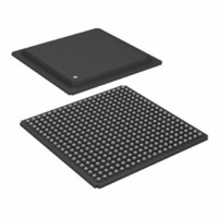
ADSP-21160NCB-100 Analog Devices Inc, ADSP-21160NCB-100 Datasheet - Page 20

ADSP-21160NCB-100
Manufacturer Part Number
ADSP-21160NCB-100
Description
IC,DSP,32-BIT,CMOS,BGA,400PIN,PLASTIC
Manufacturer
Analog Devices Inc
Series
SHARC®r
Type
Floating Pointr
Specifications of ADSP-21160NCB-100
Rohs Status
RoHS non-compliant
Interface
Host Interface, Link Port, Serial Port
Clock Rate
100MHz
Non-volatile Memory
External
On-chip Ram
512kB
Voltage - I/o
3.30V
Voltage - Core
1.90V
Operating Temperature
-40°C ~ 100°C
Mounting Type
Surface Mount
Package / Case
400-BGA
Package
400BGA
Numeric And Arithmetic Format
Floating-Point
Maximum Speed
100 MHz
Ram Size
512 KB
Device Million Instructions Per Second
100 MIPS
Lead Free Status / RoHS Status
Available stocks
Company
Part Number
Manufacturer
Quantity
Price
Company:
Part Number:
ADSP-21160NCB-100
Manufacturer:
Analog Devices Inc
Quantity:
10 000
ADSP-21160M/ADSP-21160N
TIMING SPECIFICATIONS
The ADSP-21160x DSP’s internal clock switches at higher fre-
quencies than the system input clock (CLKIN). To generate the
internal clock, the DSP uses an internal phase-locked loop
(PLL). This PLL-based clocking minimizes the skew between
the system clock (CLKIN) signal and the DSP’s internal clock
(the clock source for the external port logic and I/O pads).
The ADSP-21160x DSP’s internal clock (a multiple of CLKIN)
provides the clock signal for timing internal memory, processor
core, link ports, serial ports, and external port (as required for
read/write strobes in asynchronous access mode). During reset,
program the ratio between the DSP’s internal clock frequency
and external (CLKIN) clock frequency with the CLK_CFG3–0
pins. Even though the internal clock is the clock source for the
external port, the external port clock always switches at the
CLKIN frequency. To determine switching frequencies for the
serial and link ports, divide down the internal clock, using the
programmable divider control of each port (TDIVx/RDIVx for
the serial ports and LxCLKD1–0 for the link ports).
Note the following definitions of various clock periods that are a
function of CLKIN and the appropriate ratio control:
where:
Use the exact timing information given. Do not attempt to
derive parameters from the addition or subtraction of others.
While addition or subtraction would yield meaningful results
for an individual device, the values given in this data sheet
reflect statistical variations and worst cases. Consequently, it is
not meaningful to add parameters to derive longer times.
See
erence levels.
Switching characteristics specify how the processor changes its
signals. Circuitry external to the processor must be designed for
compatibility with these signal characteristics. Switching char-
acteristics describe what the processor will do in a given
• t
• t
• t
• LCLK = Link Port Clock
• SCLK = Serial Port Clock
• t
• t
• t
• t
• CR = Core/CLKIN Ratio (2, 3, or 4:1,
• LR = Link Port/Core Clock Ratio (1, 2, 3, or 4:1,
• SR = Serial Port/Core Clock Ratio (wide range,
Figure 33 on Page 49
determined by CLK_CFG3–0 at reset)
determined by LxCLKD)
determined by × CLKDIV)
CCLK
LCLK
SCLK
CK
CCLK
LCLK
SCLK
= CLKIN Clock Period
= (t
= (t
= Link Port Clock Period
= Serial Port Clock Period
= (t
= (Processor) Core Clock Period
CCLK
CCLK
CK
) / CR
)× SR
) × LR
under Test Conditions for voltage ref-
Rev. B | Page 20 of 60 | February 2010
circumstance. Use switching characteristics to ensure that any
timing requirement of a device connected to the processor (such
as memory) is satisfied.
Timing requirements apply to signals that are controlled by cir-
cuitry external to the processor, such as the data input for a read
operation. Timing requirements guarantee that the processor
operates correctly with other devices.
During processor reset (RESET pin low) or software reset (SRST
bit in SYSCON register = 1), deassertion (MS3–0, HBG,
DMAGx, RDx, WRx, CIF, PAGE, BRST) and three-state
(FLAG3-0, LxCLK, LxACK, LxDAT7-0, ACK, REDY, PA,
TFSx, RFSx, TCLKx, RCLKx, DTx, BMS, TDO, EMU, DATA)
timings differ. These occur asynchronously to CLKIN, and may
not meet the specifications published in the timing require-
ments and switching characteristics tables. The maximum delay
for deassertion and three-state is one t
tion low or setting the SRST bit in SYSCON. During reset the
DSP will not respond to SBTS, HBR, and MMS accesses. HBR
asserted before reset will be recognized, but an HBG will not be
returned by the DSP until after reset is deasserted and the DSP
has completed bus synchronization.
Unless otherwise noted, all timing specifications (Timing
Requirements and Switching Characteristics) listed on pages
through
Power-Up Sequencing
For power-up sequencing, see
power-up sequence of the DSP, differences in the ramp-up rates
and activation time between the two power supplies can cause
current to flow in the I/O ESD protection circuitry. To prevent
this damage to the ESD diode protection circuitry, Analog
Devices recommends including a bootstrap Schottky diode (see
Figure
V
from partially powering the V
diode will shorten the delay between the supply ramps and thus
prevent damage to the ESD diode protection circuitry. With this
technique, if the V
Schottky diode pulls the V
DDINT
9). The bootstrap Schottky diode connected between the
and V
46
apply to both ADSP-21160M and ADSP-21160N.
DDEXT
DDINT
power supplies protects the ADSP-21160x
rail rises ahead of the V
DDEXT
DDEXT
Table 12
rail along with the V
supply. Including a Schottky
CK
and
from RESET pin asser-
Figure
DDEXT
8. During the
DDINT
rail, the
rail.
21


