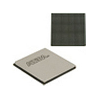
EP2SGX90EF1152I4N Altera, EP2SGX90EF1152I4N Datasheet - Page 129

EP2SGX90EF1152I4N
Manufacturer Part Number
EP2SGX90EF1152I4N
Description
Stratix II GX
Manufacturer
Altera
Datasheet
1.EP2SGX90EF1152I4N.pdf
(316 pages)
Specifications of EP2SGX90EF1152I4N
Family Name
Stratix II GX
Number Of Logic Blocks/elements
90960
# I/os (max)
558
Frequency (max)
732.1MHz
Process Technology
SRAM
Operating Supply Voltage (typ)
1.2V
Logic Cells
90960
Ram Bits
4520448
Operating Supply Voltage (min)
1.15V
Operating Supply Voltage (max)
1.25V
Operating Temp Range
-40C to 100C
Operating Temperature Classification
Industrial
Mounting
Surface Mount
Pin Count
1152
Package Type
FC-FBGA
Lead Free Status / Rohs Status
Compliant
Available stocks
Company
Part Number
Manufacturer
Quantity
Price
Company:
Part Number:
EP2SGX90EF1152I4N
Manufacturer:
ALTERA
Quantity:
535
Part Number:
EP2SGX90EF1152I4N
Manufacturer:
ALTERA/阿尔特拉
Quantity:
20 000
- Current page: 129 of 316
- Download datasheet (2Mb)
Figure 2–84. Stratix II GX IOE in DDR Output I/O Configuration
Notes to
(1)
(2)
(3)
Altera Corporation
October 2007
Column, Row,
Interconnect
or Local
All input signals to the IOE can be inverted at the IOE.
The tri-state buffer is active low. The DDIO megafunction represents the tri-state buffer as active-high with an
inverter at the OE register data port.
The optional PCI clamp is only available on column I/O pins.
ioe_clk[7..0]
Figure
2–84:
clkout
aclr/apreset
sclr/spreset
ce_out
oe
Chip-Wide Reset
Output Register
Output Register
OE Register
OE Register
ENA
CLRN/PRN
CLRN/PRN
CLRN/PRN
CLRN/PRN
D
ENA
D
ENA
D
ENA
D
Q
Q
Q
Q
Used for
DDR, DDR2
SDRAM
Notes
clk
Stratix II GX Device Handbook, Volume 1
Open-Drain Output
Drive Strength
Pin Delay
(1),
Output
Control
(2)
OE Register
t CO Delay
Stratix II GX Architecture
V CCIO
V CCIO
PCI Clamp (3)
Termination
On-Chip
Bus-Hold
Circuit
Programmable
Pull-Up
Resistor
2–121
Related parts for EP2SGX90EF1152I4N
Image
Part Number
Description
Manufacturer
Datasheet
Request
R

Part Number:
Description:
CYCLONE II STARTER KIT EP2C20N
Manufacturer:
Altera
Datasheet:

Part Number:
Description:
CPLD, EP610 Family, ECMOS Process, 300 Gates, 16 Macro Cells, 16 Reg., 16 User I/Os, 5V Supply, 35 Speed Grade, 24DIP
Manufacturer:
Altera Corporation
Datasheet:

Part Number:
Description:
CPLD, EP610 Family, ECMOS Process, 300 Gates, 16 Macro Cells, 16 Reg., 16 User I/Os, 5V Supply, 15 Speed Grade, 24DIP
Manufacturer:
Altera Corporation
Datasheet:

Part Number:
Description:
Manufacturer:
Altera Corporation
Datasheet:

Part Number:
Description:
CPLD, EP610 Family, ECMOS Process, 300 Gates, 16 Macro Cells, 16 Reg., 16 User I/Os, 5V Supply, 30 Speed Grade, 24DIP
Manufacturer:
Altera Corporation
Datasheet:

Part Number:
Description:
High-performance, low-power erasable programmable logic devices with 8 macrocells, 10ns
Manufacturer:
Altera Corporation
Datasheet:

Part Number:
Description:
High-performance, low-power erasable programmable logic devices with 8 macrocells, 7ns
Manufacturer:
Altera Corporation
Datasheet:

Part Number:
Description:
Classic EPLD
Manufacturer:
Altera Corporation
Datasheet:

Part Number:
Description:
High-performance, low-power erasable programmable logic devices with 8 macrocells, 10ns
Manufacturer:
Altera Corporation
Datasheet:

Part Number:
Description:
Manufacturer:
Altera Corporation
Datasheet:

Part Number:
Description:
Manufacturer:
Altera Corporation
Datasheet:

Part Number:
Description:
Manufacturer:
Altera Corporation
Datasheet:

Part Number:
Description:
CPLD, EP610 Family, ECMOS Process, 300 Gates, 16 Macro Cells, 16 Reg., 16 User I/Os, 5V Supply, 25 Speed Grade, 24DIP
Manufacturer:
Altera Corporation
Datasheet:


