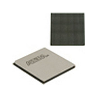
EP2SGX90EF1152I4N Altera, EP2SGX90EF1152I4N Datasheet - Page 222

EP2SGX90EF1152I4N
Manufacturer Part Number
EP2SGX90EF1152I4N
Description
Stratix II GX
Manufacturer
Altera
Datasheet
1.EP2SGX90EF1152I4N.pdf
(316 pages)
Specifications of EP2SGX90EF1152I4N
Family Name
Stratix II GX
Number Of Logic Blocks/elements
90960
# I/os (max)
558
Frequency (max)
732.1MHz
Process Technology
SRAM
Operating Supply Voltage (typ)
1.2V
Logic Cells
90960
Ram Bits
4520448
Operating Supply Voltage (min)
1.15V
Operating Supply Voltage (max)
1.25V
Operating Temp Range
-40C to 100C
Operating Temperature Classification
Industrial
Mounting
Surface Mount
Pin Count
1152
Package Type
FC-FBGA
Lead Free Status / Rohs Status
Compliant
Available stocks
Company
Part Number
Manufacturer
Quantity
Price
Company:
Part Number:
EP2SGX90EF1152I4N
Manufacturer:
ALTERA
Quantity:
535
Part Number:
EP2SGX90EF1152I4N
Manufacturer:
ALTERA/阿尔特拉
Quantity:
20 000
- Current page: 222 of 316
- Download datasheet (2Mb)
Operating Conditions
4–52
Stratix II GX Device Handbook, Volume 1
Note to
(1)
V
V
V
V
V
V
V
V
V
V
V
ΔV
V
V
V
V
V
V
V
Symbol
Table 4–39. SSTL-2 Class II Specifications
Table 4–40. SSTL-2 Class I and II Differential Specifications
Table 4–41. 1.2-V HSTL Specifications
Symbol
IH
IL
IH
IL
OH
OL
CCIO
SWING
X
SWING
ISO
OX
CCIO
REF
IH
IL
IH
IL
Symbol
ISO
(AC)
(DC)
(DC) Low-level DC input voltage
(AC)
(AC) Low-level AC input voltage
(DC)
(DC) High-level DC input voltage
(AC)
(AC) High-level AC input voltage
(AC)
This specification is supported across all the programmable drive settings available for this I/O standard as shown
in the
(DC) DC differential input voltage
(AC) AC differential input voltage
Table
Output supply voltage
Reference voltage
Stratix II GX Architecture
High-level DC input voltage
Low-level DC input voltage
High-level AC input voltage
Low-level AC input voltage
High-level output voltage
Low-level output voltage
Output supply voltage
AC differential input cross
point voltage
Input clock signal offset
voltage
Input clock signal offset
voltage variation
AC differential output cross
point voltage
4–39:
Parameter
Parameter
Parameter
chapter in volume 1 of the Stratix II GX Device Handbook.
Conditions
I
I
OH
OL
Conditions
= 16.4 mA
Conditions
= –16.4 mA
V
V
0.48 V
Minimum
(1)
REF
REF
(V
(V
(1)
–0.15
–0.24
1.14
Minimum
CCIO
CCIO
+ 0.08
+ 0.15
2.375
CCIO
V
V
0.36
V
0.7
Minimum
/2) – 0.2
/2) – 0.2
REF
REF
TT
–0.3
+ 0.76
+ 0.18
+ 0.35
0.5 V
Typical
0.5 V
1.2
Typical
2.5
200
CCIO
Typical
CCIO
(V
(V
V
V
V
V
Maximum
0.52 V
CCIO
CCIO
Maximum
CCIO
CCIO
REF
REF
Altera Corporation
V
V
V
Maximum
V
2.625
1.26
REF
REF
CCIO
TT
/2) + 0.2
/2) + 0.2
– 0.08
– 0.15
+ 0.15
+ 0.24
CCIO
– 0.76
– 0.18
– 0.35
+ 0.3
June 2009
Unit
Unit
Unit
mV
V
V
V
V
V
V
V
V
V
V
V
V
V
V
V
V
V
V
Related parts for EP2SGX90EF1152I4N
Image
Part Number
Description
Manufacturer
Datasheet
Request
R

Part Number:
Description:
CYCLONE II STARTER KIT EP2C20N
Manufacturer:
Altera
Datasheet:

Part Number:
Description:
CPLD, EP610 Family, ECMOS Process, 300 Gates, 16 Macro Cells, 16 Reg., 16 User I/Os, 5V Supply, 35 Speed Grade, 24DIP
Manufacturer:
Altera Corporation
Datasheet:

Part Number:
Description:
CPLD, EP610 Family, ECMOS Process, 300 Gates, 16 Macro Cells, 16 Reg., 16 User I/Os, 5V Supply, 15 Speed Grade, 24DIP
Manufacturer:
Altera Corporation
Datasheet:

Part Number:
Description:
Manufacturer:
Altera Corporation
Datasheet:

Part Number:
Description:
CPLD, EP610 Family, ECMOS Process, 300 Gates, 16 Macro Cells, 16 Reg., 16 User I/Os, 5V Supply, 30 Speed Grade, 24DIP
Manufacturer:
Altera Corporation
Datasheet:

Part Number:
Description:
High-performance, low-power erasable programmable logic devices with 8 macrocells, 10ns
Manufacturer:
Altera Corporation
Datasheet:

Part Number:
Description:
High-performance, low-power erasable programmable logic devices with 8 macrocells, 7ns
Manufacturer:
Altera Corporation
Datasheet:

Part Number:
Description:
Classic EPLD
Manufacturer:
Altera Corporation
Datasheet:

Part Number:
Description:
High-performance, low-power erasable programmable logic devices with 8 macrocells, 10ns
Manufacturer:
Altera Corporation
Datasheet:

Part Number:
Description:
Manufacturer:
Altera Corporation
Datasheet:

Part Number:
Description:
Manufacturer:
Altera Corporation
Datasheet:

Part Number:
Description:
Manufacturer:
Altera Corporation
Datasheet:

Part Number:
Description:
CPLD, EP610 Family, ECMOS Process, 300 Gates, 16 Macro Cells, 16 Reg., 16 User I/Os, 5V Supply, 25 Speed Grade, 24DIP
Manufacturer:
Altera Corporation
Datasheet:


