KMA199,115 NXP Semiconductors, KMA199,115 Datasheet
KMA199,115
Specifications of KMA199,115
Available stocks


Related parts for KMA199,115


KMA199,115 Summary of contents
Page 1
KMA199 Programmable angle sensor Rev. 01 — 26 April 2010 1. Product profile 1.1 General description The KMA199 is a magnetic angle sensor system. The MagnetoResistive (MR) sensor bridges and the mixed signal Integrated Circuit (IC) are integrated into a ...
Page 2
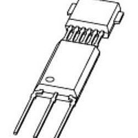
... NXP Semiconductors 2. Pinning information Table 1. Pin Symbol GND 3 OUT/DATA 3. Ordering information Table 2. Type number KMA199 KMA199_1 Product data sheet Pinning Description supply voltage DD ground analog output or data interface Ordering information Package Name Description - plastic single-ended multi-chip package; 6 interconnections; 3 in-line leads All information provided in this document is subject to legal disclaimers. ...
Page 3
ref DDS I REGULATOR REGULATOR ref V V SSE DDS V SINP MUX AMPLIFIER V SINN COSP V COSN V SSS TP0 TP1 TP2 DIGITAL FILTER TEST CONTROL AND AVERAGING Q_PUMP ARRAY EEPROM ...
Page 4
... NXP Semiconductors 5. Functional description The KMA199 amplifies two orthogonal differential signals which are delivered by MR sensor bridges and converts them into the digital domain. The angle is calculated using the COordinate Rotation DIgital Computer (CORDIC) algorithm. After a digital-to-analog conversion the analog signal is provided to the output. Thus, the output is a linear representation of the angular value ...
Page 5
... NXP Semiconductors Fig 2. Since the Anisotropic MR (AMR) effect is periodic over 180°, the sensor output is also 180°-periodic, where the angle is calculated relative to a freely programmable zero angle. The dashed line indicates the mechanical zero degree position. 6. Analog output The KMA199 provides one analog output signal on pin OUT/DATA. The measured angle α ...
Page 6
... NXP Semiconductors Fig 3. 7. Diagnostic features The KMA199 provides four diagnostic features: 7.1 EEPROM CRC and EDC supervision The KMA199 system includes a supervision of the programmed data. At power-on, a CRC of the EEPROM is performed. Furthermore the EEPROM is protected against bit errors. Every 16-bit data word is saved internally as a 22-bit word for this purpose. The protection logic corrects any single-bit error in a data word, while the sensor continues in normal operation mode ...
Page 7
... NXP Semiconductors Fig 4. Equivalent output circuit in case of a power-loss condition Table 4 resistance. Table 4. Load resistance R > 5 kΩ L 7.4 Low supply voltage detection If the supply voltage is below the switch-off threshold voltage, a status bit is set. Table 5 Table 5. Voltage range ≈ 1.5 V ≈ 1 ...
Page 8
... NXP Semiconductors 8. Limiting values Table 6. In accordance with the Absolute Maximum Rating System (IEC 60134). Symbol amb T amb(pr) T stg EEPROM t ret(D) N endu(W_ER) [1] Time until sensor environment is initialized. [2] The maximum value of the output voltage is 5 Recommended operating conditions Table homogenous magnetic field. ...
Page 9
... NXP Semiconductors 11. Characteristics Table 9. Supply current Characteristics are valid for the operating conditions, as specified in Symbol Parameter I supply current DD [1] Normal operating mode. [2] Without load current at the analog output. Table 10. Power-on reset Characteristics are valid for the operating conditions, as specified in Symbol Parameter ...
Page 10
... NXP Semiconductors Table 11. System performance Characteristics are valid for the operating conditions, as specified in Symbol Parameter Δφ temperature drift error at temp⏐RT room temperature Δφ hysteresis error hys Δφ microlinearity error μlin Δφ angular error ang m slope of angular error ...
Page 11
... NXP Semiconductors 1.40 1. ang (deg) 1.10 0.75 0. (1) −40 °C to +160 °C. (2) −40 °C to +140 °C. Fig 5. Envelope curve for the magnitude of angular error Table 12. Dynamics Characteristics are valid for the operating conditions, as specified in Symbol Parameter t turn-on time on f update frequency ...
Page 12
... NXP Semiconductors Table 13. Digital interface …continued Characteristics are valid for the operating conditions, as specified in Symbol Parameter t stop time stop T bit period bit ΔT bit period deviation bit t pulse width pulse width time-out time to t slave takeover time tko(slv) t master takeover time ...
Page 13
... NXP Semiconductors 12.2 Hysteresis error The hysteresis error Δφ given by the device output when performing a positive (clockwise) rotation and negative (counter clockwise) rotation over an angular range of 180°, measured at a constant temperature. Fig 7. Definition of the hysteresis error Equation 1 Δ φ ...
Page 14
... NXP Semiconductors 12.4 Microlinearity error The microlinearity error Δφ angle α is changed by Δα = 1°. Fig 9. Definition of the microlinearity error 12.5 Temperature drift error The temperature drift Δφ versus the temperature range considered as the pure thermal effect. Fig 10. Definition of the temperature drift error Equation 2 Δ ...
Page 15
... NXP Semiconductors The deviation from the value at room temperature Δφ drift of the angle, compared to the value, which the sensor provides at room temperature: Δφ temp RT with: : room temperature (25 ° 12.6 Angular error The angular error Δφ mechanical angle deviates from α ...
Page 16
... NXP Semiconductors Angular error can be expressed by − α for |α 1 Δ φ ang for 1° < |α Δ φ ang − α for |α 1 Δ φ ang with: Δ α ∗ = ---------------------------------------------------------------------------------- - 13. Programming 13.1 General description The KMA199 provides an OWI to enable programming of the device which uses pin OUT/DATA bidirectionally ...
Page 17
... NXP Semiconductors During communication, the KMA199 is always the slave and the external programming hardware is the master. Fig 12. OWI data format The master provides the start condition, which is a rising edge after a LOW level. Then a command byte which can be either a read or a write command is send. Depending on the command, the master or the slave has to send the data immediately after the command sequence ...
Page 18
... NXP Semiconductors Figure 14 Here the pulse width t respectively. Fig 14. OWI timing 13.3 Sending and receiving data The master has to control the communication during sending or receiving data. The command byte defines the region, address and type of command requested by the master. In case of a read command, an additional handover or takeover bit must be inserted before and after the two data bytes (see data transmission, whereas the Most Significant Byte (MSB) must be send at first ...
Page 19
... NXP Semiconductors 13.3.1 Write access To write data to the EEPROM, the internal charge pump must be enabled by setting the bits EEP_CP_CLOCK_EN and EEP_WRITE_EN and waiting for t procedure must be performed: • Start condition: The master drives a rising edge after a LOW level • Command: The master sends a write command (CMD0 = 0) • ...
Page 20
... NXP Semiconductors 13.3.2 Read access To read data from the sensor, the following procedure must be performed: • Start condition: The master drives a rising edge after a LOW level • Command: The master sends a read command (CMD0 = 1) • Handover: The master sends a handover bit, that is a logic 0 and disables the output after a three-quarter bit period • ...
Page 21
... NXP Semiconductors 13.3.3 Entering the command mode After a power-on reset, the sensor provides a time slot t mode. A specific command sequence has to be send (see is not entered, the sensor starts in the normal operating mode. However the signature can be written by the master, if the sensor switches to diagnostic mode. ...
Page 22
... NXP Semiconductors 13.4.1 Software example #include <stdio.h.> calc_crc accepts unsigned 16-bit data in data 4 int calc_crc(int crc, unsigned int data const int gpoly = 0x107; // generator polynomial 7 int i; 8 for (i = 15; i >= 0; i--) crc <<= 1; crc |= (int) ((data & (1u<<i))>>i XOR of with generator polynomial when MSB(9) = HIGH 13 if (crc & ...
Page 23
... NXP Semiconductors 13.5 Registers 13.5.1 Command registers To enter the command mode, the signature given in OWI into the specific register. This must be done as described in write command, followed by the signature, but after a power-on reset and not later than t cmd(ent) Table 16. Command registers Command ...
Page 24
... NXP Semiconductors 13.5.2 EEPROM registers The device includes several internal registers which are used for customization and identification. The initial signature allows read access to all areas but only write access to customer registers. Write accesses to reserved areas are ignored. Since these registers are implemented as EEPROM cells, writing to the registers needs a specific time t each write access to complete ...
Page 25
... NXP Semiconductors Table 17. EEPROM registers …continued Address Command Register write/read Fh 1Eh/1Fh EEP_CTRL_CUST [1] Variable and individual for each device. [2] Undefined; must be written as zero for default. Table 18. ZERO_ANGLE - mechanical zero degree position (address 7h) bit allocation Data format: unsigned fixed point; resolution: 2 Bit 15 14 ...
Page 26
... NXP Semiconductors Table 20. CLAMP_LO - lower clamping level output voltage (address Ah) bit allocation Data format: integer (DAC values 256 to 4 864); resolution: 2 Bit [1] [1] [1] Value [1] Undefined; must be written as zero for default and may return any value when read. Values 0 to 255 are reserved not permitted to use such values. ...
Page 27
... NXP Semiconductors CLAMP_SW_ANGLE If the magnetic field angle is larger than the CLAMP_SW_ANGLE, the output switches to CLAMP_LO for a positive slope. The value of CLAMP_SW_ANGLE can be calculated from other EEPROM constants but must be programmed. 14. Electromagnetic compatibility EMC is verified in an independent and certified test laboratory. 14.1 Emission (CISPR 25) Tests according to CISPR 25 were fulfilled ...
Page 28
... NXP Semiconductors 14.2.2 Bulk-current injection Tests according to ISO 11452-4, third edition (2005-04), were fulfilled. Test level: 200 mA with C State: A. 14.2.3 Strip line Tests according to ISO 11452-5, second edition (2002-04), were fulfilled. Test level: 200 V/m with C State: A. 14.2.4 Immunity against mobile phones Tests according to ISO 11452-2, second edition (2004-11), were fulfilled ...
Page 29
... NXP Semiconductors 15. ElectroStatic Discharge (ESD) To raise immunity against ESD pulses, protection diodes are implemented into the KMA199. 15.1 Human body model The KMA199 must not be damaged at 8 kV, according to the human body model at 100 pF and 1.5 kΩ. The test is according to AEC-Q100-002, CLASS H3A. This protection ...
Page 30
... NXP Semiconductors 16. Application information (1) The block capacitance C (2) The load capacitance C Fig 18. Application diagram of KMA199 17. Test information 17.1 Quality information This product has been qualified in accordance with the Automotive Electronics Council (AEC) standard Q100 - Failure mechanism based stress test qualification for integrated circuits, and is suitable for use in automotive applications ...
Page 31
... NXP Semiconductors 18. Marking Fig 19. Marking 19. Terminals Lead frame material: CuZr with 99 and 0 Lead finish: matt tin; thickness 8 μ μm KMA199_1 Product data sheet 2.1 min X Marking paint: laser Code: see drawing Type face: DIN 1451 condensed type Letter height: 0.8 mm Line spacing: 0.25 mm Crossing of lines not allowed A: leading letters of type number (5 characters max ...
Page 32
... NXP Semiconductors 20. Package outline Plastic single-ended multi-chip package; 6 interconnections; 3 in-line leads (1) (1) A (1) 1 DIMENSIONS (mm are the original dimensions UNIT 1.65 0.41 1.57 0.30 4.1 mm 1.45 0.34 1.47 0.24 3.9 Note 1. Terminals within this zone are uncontrolled to allow for flow of plastic between and besides the leads. ...
Page 33
... NXP Semiconductors 21. Handling information (1) No bending allowed. (2) Plastic body and interface plastic body - leads: application of bending forces not allowed. Fig 21. Bending recommendation 22. Solderability information The solderability qualification is done according to AEC-Q100, Rev-F. Recommended soldering process for leaded devices is wave soldering. The maximum soldering temperature is 260 ° ...
Page 34
... In no event shall NXP Semiconductors be liable for any indirect, incidental, punitive, special or consequential damages (including - without limitation - lost profits, lost savings, business interruption, costs related to the removal or ...
Page 35
... NXP Semiconductors 25. Contact information For more information, please visit: For sales office addresses, please send an email to: KMA199_1 Product data sheet http://www.nxp.com salesaddresses@nxp.com All information provided in this document is subject to legal disclaimers. Rev. 01 — 26 April 2010 KMA199 Programmable angle sensor © NXP B.V. 2010. All rights reserved. ...
Page 36
... NXP Semiconductors 26. Contents 1 Product profile . . . . . . . . . . . . . . . . . . . . . . . . . . 1 1.1 General description . . . . . . . . . . . . . . . . . . . . . 1 1.2 Features and benefits . . . . . . . . . . . . . . . . . . . . 1 2 Pinning information . . . . . . . . . . . . . . . . . . . . . . 2 3 Ordering information . . . . . . . . . . . . . . . . . . . . . 2 4 Functional diagram . . . . . . . . . . . . . . . . . . . . . . 3 5 Functional description . . . . . . . . . . . . . . . . . . . 4 5.1 Angular measurement directions . . . . . . . . . . . 4 6 Analog output Diagnostic features . . . . . . . . . . . . . . . . . . . . . . 6 7.1 EEPROM CRC and EDC supervision 7.2 Magnet-loss detection . . . . . . . . . . . . . . . . . . . 6 7 ...