HGT1S10N120BNS Fairchild Semiconductor, HGT1S10N120BNS Datasheet - Page 2
HGT1S10N120BNS
Manufacturer Part Number
HGT1S10N120BNS
Description
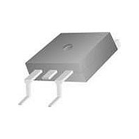
IGBT NPT N-CHAN 1200V TO-263AB
Manufacturer
Fairchild Semiconductor
Datasheet
1.HGT1S10N120BNST.pdf
(8 pages)
Specifications of HGT1S10N120BNS
Igbt Type
NPT
Voltage - Collector Emitter Breakdown (max)
1200V
Vce(on) (max) @ Vge, Ic
2.7V @ 15V, 10A
Current - Collector (ic) (max)
35A
Power - Max
298W
Input Type
Standard
Mounting Type
Surface Mount
Package / Case
D²Pak, TO-263 (2 leads + tab)
Configuration
Single
Collector- Emitter Voltage Vceo Max
1200 V
Collector-emitter Saturation Voltage
2.7 V
Maximum Gate Emitter Voltage
+/- 20 V
Continuous Collector Current At 25 C
35 A
Gate-emitter Leakage Current
+/- 250 nA
Power Dissipation
298 W
Maximum Operating Temperature
+ 150 C
Continuous Collector Current Ic Max
35 A
Minimum Operating Temperature
- 55 C
Mounting Style
SMD/SMT
Lead Free Status / RoHS Status
Lead free / RoHS Compliant
Available stocks
Company
Part Number
Manufacturer
Quantity
Price
Company:

Part Number:
HGT1S10N120BNS
Manufacturer:
FAIRCHILD
Quantity:
12 500
Part Number:
HGT1S10N120BNS
Manufacturer:
FAIRCHILD/仙童
Quantity:
20 000
Part Number:
HGT1S10N120BNST
Manufacturer:
FAIRCHILD/仙童
Quantity:
20 000


Absolute Maximum Ratings
Collector to Emitter Voltage . . . . . . . . . . . . . . . . . . . . . . . . . . . . . . . . . . . . . . . . . . . . . .BV
Collector Current Continuous
Collector Current Pulsed (Note 1) . . . . . . . . . . . . . . . . . . . . . . . . . . . . . . . . . . . . . . . . . . . I
Gate to Emitter Voltage Continuous. . . . . . . . . . . . . . . . . . . . . . . . . . . . . . . . . . . . . . . . . V
Gate to Emitter Voltage Pulsed . . . . . . . . . . . . . . . . . . . . . . . . . . . . . . . . . . . . . . . . . . . .V
Switching Safe Operating Area at T
Power Dissipation Total at T
Power Dissipation Derating T
Forward Voltage Avalanche Energy (Note 2) . . . . . . . . . . . . . . . . . . . . . . . . . . . . . . . . . . . E
Operating and Storage Junction Temperature Range . . . . . . . . . . . . . . . . . . . . . . . . T
Maximum Temperature for Soldering
Short Circuit Withstand Time (Note 3) at V
Short Circuit Withstand Time (Note 3) at V
CAUTION: Stresses above those listed in “Absolute Maximum Ratings” may cause permanent damage to the device. This is a stress only rating and operation of the
device at these or any other conditions above those indicated in the operational sections of this specification is not implied.
NOTES:
Electrical Specifications
©2002 Fairchild Semiconductor Corporation
Collector to Emitter Breakdown Voltage
Emitter to Collector Breakdown Voltage
Collector to Emitter Leakage Current
Collector to Emitter Saturation Voltage
Gate to Emitter Threshold Voltage
Gate to Emitter Leakage Current
Switching SOA
Gate to Emitter Plateau Voltage
On-State Gate Charge
1. Pulse width limited by maximum junction temperature.
2. I
3. V
At T
At T
Leads at 0.063in (1.6mm) from Case for 10s. . . . . . . . . . . . . . . . . . . . . . . . . . . . . . . . . . T
Package Body for 10s, see Tech Brief 334. . . . . . . . . . . . . . . . . . . . . . . . . . . . . . . . . . .T
CE
CE(PK)
C
C
= 25
= 110
= 20A, L = 400 H, T
o
= 840V, T
C . . . . . . . . . . . . . . . . . . . . . . . . . . . . . . . . . . . . . . . . . . . . . . . . . . . . . . . . . I
o
PARAMETER
C . . . . . . . . . . . . . . . . . . . . . . . . . . . . . . . . . . . . . . . . . . . . . . . . . . . . . . . I
J
= 125
C
J
C
= 25
= 25
o
> 25
C, R
o
o
J
C . . . . . . . . . . . . . . . . . . . . . . . . . . . . . . . . . . . . . . . . . P
o
T
C.
G
C . . . . . . . . . . . . . . . . . . . . . . . . . . . . . . . . . . . . . . . . . .
= 150
C
T
= 10
= 25
C
= 25
GE
GE
o
o
C (Figure 2) . . . . . . . . . . . . . . . . . . . . . . . SSOA
C, Unless Otherwise Specified
= 15V. . . . . . . . . . . . . . . . . . . . . . . . . . . . . .t
= 12V. . . . . . . . . . . . . . . . . . . . . . . . . . . . . .t
o
C, Unless Otherwise Specified
SYMBOL
V
V
Q
BV
BV
CE(SAT)
SSOA
GE(TH)
V
I
I
G(ON)
GES
CES
GEP
CES
ECS
I
I
V
I
V
I
V
T
L = 400 H, V
I
I
V
C
C
C
C
C
C
GE
GE
J
CE
CE
= 250 A, V
= 10mA, V
= 10A,
= 90 A, V
= 10A, V
= 10A,
= 150
= 1200V
= 15V
= 20V
= 600V
o
TEST CONDITIONS
C, R
CE
CE
CE(PK)
GE
GE
G
= 600V
= V
=
= 0V
= 0V
GE
= 1200V
T
T
T
T
T
V
V
J
, T
C
C
C
C
C
GE
GE
V
C110
GEM
= 25
= 125
= 150
= 25
= 150
GES
CES
STG
GE
C25
pkg
CM
= 15V
= 20V
SC
SC
AV
D
L
= 15V,
o
o
C
C
o
o
o
C
C
C
HGTG10N120BN, HGTP10N120BN, HGT1S10N120BNS Rev. B1
HGT1S10N120BNS
HGTG10N120BN
HGTP10N120BN
55A at 1200V
-55 to 150
1200
MIN
6.0
15
55
1200
2.38
298
300
260
-
-
-
-
-
-
-
-
-
35
17
80
80
15
20
30
8
TYP
2.45
10.4
150
100
130
3.7
6.8
-
-
-
-
-
-
MAX
250
120
150
2.7
4.2
250
2
-
-
-
-
-
-
UNITS
W/
mJ
o
o
o
W
V
A
A
A
V
V
C
C
C
UNITS
o
s
s
C
mA
nC
nC
nA
V
V
V
V
V
A
V
A
A
Related parts for HGT1S10N120BNS
Image
Part Number
Description
Manufacturer
Datasheet
Request
R

Part Number:
Description:
Fairchild Semiconductor [IGBT MODULE]
Manufacturer:
Fairchild Semiconductor
Datasheet:

Part Number:
Description:
Discrete Semiconductor Modules
Manufacturer:
Fairchild Semiconductor
Part Number:
Description:
Discrete Semiconductor Modules
Manufacturer:
Fairchild Semiconductor
Part Number:
Description:
This N-Channel MOSFET is produced using Fairchild Semiconductor’s advanced Power Trench® process
Manufacturer:
Fairchild Semiconductor
Datasheet:
Part Number:
Description:
This N-Channel MOSFET is produced using Fairchild Semiconductor’s advanced Power Trench® process
Manufacturer:
Fairchild Semiconductor
Datasheet:
Part Number:
Description:
This N-Channel MOSFET is produced using Fairchild Semiconductor’s advanced PowerTrench® process
Manufacturer:
Fairchild Semiconductor
Datasheet:
Part Number:
Description:
This N-Channel MOSFET is produced using Fairchild Semiconductor’s advanced PowerTrench® process
Manufacturer:
Fairchild Semiconductor
Datasheet:
Part Number:
Description:
This N-Channel MOSFET is produced using Fairchild Semiconductor’s advanced Power Trench® process
Manufacturer:
Fairchild Semiconductor
Datasheet:
Part Number:
Description:
This N-Channel logic Level MOSFETs are produced using Fairchild Semiconductor‘s advanced Power Trench® process that has been special tailored to minimize the on-state resistance and yet maintain superior switching performance
Manufacturer:
Fairchild Semiconductor
Datasheet:
Part Number:
Description:
This N-Channel MOSFET is produced using Fairchild Semiconductor’s advanced Power Trench® process
Manufacturer:
Fairchild Semiconductor
Datasheet:
Part Number:
Description:
This N-Channel SyncFET™ is produced using Fairchild Semiconductor’s advanced PowerTrench® process
Manufacturer:
Fairchild Semiconductor
Datasheet:
Part Number:
Description:
This N-Channel SyncFET™ is produced using Fairchild Semiconductor’s advanced PowerTrench® process
Manufacturer:
Fairchild Semiconductor
Datasheet:
Part Number:
Description:
This N-Channel SyncFET™ is produced using Fairchild Semiconductor’s advanced PowerTrench® process
Manufacturer:
Fairchild Semiconductor
Datasheet:
Part Number:
Description:
This N-Channel logic Level MOSFETs are produced using Fairchild Semiconductor‘s advanced Power Trench® process that has been special tailored to minimize the on-state resistance and yet maintain superior switching performance
Manufacturer:
Fairchild Semiconductor
Datasheet:
Part Number:
Description:
This N-Channel MOSFET is produced using Fairchild Semiconductor’s advanced Power Trench® process that has been especially tailored to minimize the on-state resistance and yet maintain superior switching performance
Manufacturer:
Fairchild Semiconductor
Datasheet: