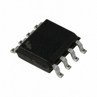
NDS9430 Fairchild Semiconductor, NDS9430 Datasheet - Page 4

NDS9430
Manufacturer Part Number
NDS9430
Description
MOSFET P-CH 30V 5.3A 8-SOIC
Manufacturer
Fairchild Semiconductor
Series
PowerTrench®r
Datasheet
1.NDS9430.pdf
(5 pages)
Specifications of NDS9430
Fet Type
MOSFET P-Channel, Metal Oxide
Fet Feature
Logic Level Gate
Rds On (max) @ Id, Vgs
60 mOhm @ 5.3A, 10V
Drain To Source Voltage (vdss)
30V
Current - Continuous Drain (id) @ 25° C
5.3A
Vgs(th) (max) @ Id
3V @ 250µA
Gate Charge (qg) @ Vgs
14nC @ 10V
Input Capacitance (ciss) @ Vds
528pF @ 15V
Power - Max
1W
Mounting Type
Surface Mount
Package / Case
8-SOIC (3.9mm Width)
Lead Free Status / RoHS Status
Lead free / RoHS Compliant
Other names
NDS9430TR
Available stocks
Company
Part Number
Manufacturer
Quantity
Price
Part Number:
NDS9430
Manufacturer:
FAIRCHILD/仙童
Quantity:
20 000
Part Number:
NDS9430-NL
Manufacturer:
FAIRCHILD/仙童
Quantity:
20 000
Company:
Part Number:
NDS9430A
Manufacturer:
FSC
Quantity:
5 510
Company:
Part Number:
NDS9430A
Manufacturer:
FSC
Quantity:
1 310
Part Number:
NDS9430A
Manufacturer:
FAIRCHILD/仙童
Quantity:
20 000
Part Number:
NDS9430A-NL
Manufacturer:
FAIRCHILD/仙童
Quantity:
20 000
Typical Characteristics
0.01
10
100
0.1
8
6
4
2
0
10
Figure 9. Maximum Safe Operating Area.
1
0
Figure 7. Gate Charge Characteristics.
0.1
0.001
I
0.01
D
R
SINGLE PULSE
R
0.1
= -5.3A
DS(ON)
0.0001
V
JA
1
T
GS
A
= 125
= 25
= -10V
LIMIT
D = 0.5
2
o
o
0.2
C
0.1
C/W
0.05
0.02
-V
0.01
DS
, DRAIN-SOURCE VOLTAGE (V)
Q
1
g
, GATE CHARGE (nC)
SINGLE PULSE
4
0.001
DC
10s
1s
Figure 11. Transient Thermal Response Curve.
100ms
6
Thermal characterization performed using the conditions described in Note 1c.
Transient thermal response will change depending on the circuit board design.
10ms
V
DS
10
= -5V
1ms
0.01
100 s
8
-15V
-10V
100
10
0.1
t
1
, TIME (sec)
800
700
600
500
400
300
200
100
50
40
30
20
10
0
0
0.001
0
Figure 8. Capacitance Characteristics.
C
Figure 10. Single Pulse Maximum
RSS
1
0.01
5
C
-V
OSS
DS
Power Dissipation.
, DRAIN TO SOURCE VOLTAGE (V)
0.1
10
C
t
1
10
ISS
, TIME (sec)
15
1
Duty Cycle, D = t
P(pk)
T
R
10
20
J
R
JA
- T
JA
(t) = r(t) + R
100
A
SINGLE PULSE
R
= 125
= P * R
t
JA
1
T
t
A
100
2
= 125°C/W
25
= 25°C
o
C/W
f = 1 MHz
V
NDS9430 Rev B
GS
JA
1
= 0 V
(t)
JA
/ t
2
1000
30
1000


