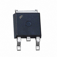
FDD4141 Fairchild Semiconductor, FDD4141 Datasheet - Page 2

FDD4141
Manufacturer Part Number
FDD4141
Description
MOSFET P-CH 40V 10.8A DPAK
Manufacturer
Fairchild Semiconductor
Series
PowerTrench®r
Type
Power MOSFETr
Datasheet
1.FDD4141.pdf
(6 pages)
Specifications of FDD4141
Fet Type
MOSFET P-Channel, Metal Oxide
Fet Feature
Logic Level Gate
Rds On (max) @ Id, Vgs
12.3 mOhm @ 12.7A, 10V
Drain To Source Voltage (vdss)
40V
Current - Continuous Drain (id) @ 25° C
10.8A
Vgs(th) (max) @ Id
3V @ 250µA
Gate Charge (qg) @ Vgs
50nC @ 10V
Input Capacitance (ciss) @ Vds
2775pF @ 20V
Power - Max
2.4W
Mounting Type
Surface Mount
Package / Case
DPak, TO-252 (2 leads+tab), SC-63
Configuration
Single
Transistor Polarity
P-Channel
Resistance Drain-source Rds (on)
12.3 Ohm @ 10 V
Drain-source Breakdown Voltage
40 V
Gate-source Breakdown Voltage
+/- 20 V
Continuous Drain Current
10.8 A
Power Dissipation
2400 mW
Maximum Operating Temperature
+ 150 C
Mounting Style
SMD/SMT
Minimum Operating Temperature
- 55 C
Number Of Elements
1
Polarity
P
Channel Mode
Enhancement
Drain-source On-res
12.3Ohm
Drain-source On-volt
40V
Gate-source Voltage (max)
±20V
Operating Temp Range
-55C to 150C
Operating Temperature Classification
Military
Mounting
Surface Mount
Pin Count
2 +Tab
Package Type
TO-252
Lead Free Status / RoHS Status
Lead free / RoHS Compliant
Other names
FDD4141
FDD4141TR
FDD4141TR
Available stocks
Company
Part Number
Manufacturer
Quantity
Price
Company:
Part Number:
FDD4141
Manufacturer:
Fairchild Semiconductor
Quantity:
33 824
Part Number:
FDD4141
Manufacturer:
FAIRCHILD/仙童
Quantity:
20 000
Part Number:
FDD4141-F085
Manufacturer:
ON/安森美
Quantity:
20 000
©2007 Fairchild Semiconductor Corporation
FDD4141 Rev.C
Electrical Characteristics
Off Characteristics
On Characteristics
Dynamic Characteristics
Switching Characteristics
Drain-Source Diode Characteristics
Notes:
1: R
2: Pulse Test: Pulse Width < 300µs, Duty cycle < 2.0%.
3: Starting T
BV
∆BV
I
I
V
r
g
C
C
C
R
t
t
t
t
Q
Q
Q
Q
V
t
Q
∆V
DSS
GSS
d(on)
r
d(off)
f
rr
DS(on)
FS
GS(th)
SD
iss
oss
rss
g
∆T
∆T
g
g
gs
gd
rr
R
Symbol
DSS
θJA
θJC
GS(th)
DSS
J
J
is the sum of the junction-to-case and case-to-ambient thermal resistance where the case thermal reference is defined as the solder mounting surface of the drain pins.
is guaranteed by design while R
J
= 25
Drain to Source Breakdown Voltage
Breakdown Voltage Temperature
Coefficient
Zero Gate Voltage Drain Current
Gate to Source Leakage Current
Gate to Source Threshold Voltage
Gate to Source Threshold Voltage
Temperature Coefficient
Static Drain to Source On Resistance
Forward Transconductance
Input Capacitance
Output Capacitance
Reverse Transfer Capacitance
Gate Resistance
Turn-On Delay Time
Rise Time
Turn-Off Delay Time
Fall Time
Total Gate Charge
Total Gate Charge
Gate to Source Charge
Gate to Drain “Miller” Charge
Source to Drain Diode Forward Voltage
Reverse Recovery Time
Reverse Recovery Charge
°
C, L = 3mH, I
AS
= 15A, V
Parameter
θJA
DD
is determined by the user’s board design.
= 40V, V
T
a)
GS
J
= 25°C unless otherwise noted
1 in
= 10V.
52°C/W when mounted on a
2
pad of 2 oz copper
V
V
V
V
V
f = 1MHz
f = 1MHz
V
I
V
V
V
T
V
V
I
I
I
V
V
D
F
D
D
DD
GS
GS
GS
GS
GS
GS
GS
J
DS
DS
GS
DS
GS
= -12.7A, di/dt = 100A/µs
= -250µA, referenced to 25°C
= -250µA, V
= -250µA, referenced to 25°C
= 125°C
= 0V to -10V
= 0V to -5V
= -20V, V
= -20V, I
= -10V, R
= -5V, I
= 0V, I
= -32V, V
= V
= -10V, I
= -4.5V, I
= -10V, I
= ±20V, V
2
DS
Test Conditions
, I
S
D
D
D
= -12.7A
D
D
D
= -12.7A
GS
GEN
GS
= -250µA
GS
= -12.7A,
DS
= -12.7A
= -12.7A,
= -10.4A
= 0V,
= 0V
= 0V
= 0V
= 6Ω
V
I
D
DD
= -12.7A
= -20V,
(Note 2)
b)
100°C/W when mounted
on a minimum pad.
Min
-40
-1
2085
10.1
14.5
15.3
-0.8
-1.8
360
210
4.6
Typ
5.8
29
26
10
38
15
36
19
38
-29
7
7
8
2775
±100
12.3
18.0
18.7
-1.2
Max
480
310
19
13
60
27
50
27
44
40
-3
www.fairchildsemi.com
-1
mV/°C
mV/°C
Units
mΩ
nC
pF
pF
pF
nC
nC
nC
nC
µA
nA
ns
ns
ns
ns
ns
Ω
V
V
S
V


