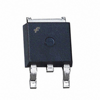
HUFA75429D3ST Fairchild Semiconductor, HUFA75429D3ST Datasheet

HUFA75429D3ST
Specifications of HUFA75429D3ST
Related parts for HUFA75429D3ST
HUFA75429D3ST Summary of contents
Page 1
... This product has been designed to meet the extreme test conditions and environment demanded by the automotive industry. For a copy of the requirements, see AEC Q101 at: http://www.aecouncil.com/ Reliability data can be found at: http://www.fairchildsemi.com/products/discrete/reliability/index.html. All Fairchild Semiconductor products are manufactured, assembled and tested under ISO9000 and QS9000 quality systems certifi- ©2003 Fairchild Semiconductor Corporation Applications • ...
Page 2
... Package Marking and Ordering Information Device Marking Device 75429D HUFA75429D3ST 75429D HUFA75429D3S Electrical Characteristics Symbol Parameter Off Characteristics B Drain to Source Breakdown Voltage VDSS I Zero Gate Voltage Drain Current DSS I Gate to Source Leakage Current GSS On Characteristics V Gate to Source Threshold Voltage GS(TH) r Drain to Source On Resistance ...
Page 3
... SINGLE PULSE 0. Figure 3. Normalized Maximum Transient Thermal Impedance 600 V = 10V GS 100 TRANSCONDUCTANCE MAY LIMIT CURRENT IN THIS REGION ©2003 Fairchild Semiconductor Corporation T = 25°C unless otherwise noted 150 175 125 Figure 2. Maximum Continuous Drain Current RECTANGULAR PULSE DURATION ( ...
Page 4
... GS Figure 7. Transfer Characteristics 2.5 PULSE DURATION = 80 s DUTY CYCLE = 0.5% MAX 2.0 1.5 1.0 0.5 -80 - JUNCTION TEMPERATURE ( J Figure 9. Normalized Drain to Source On Resistance vs Junction Temperature ©2003 Fairchild Semiconductor Corporation T = 25°C unless otherwise noted A 500 100 s AV 100 1ms 10 10ms STARTING T 1 0.01 100 NOTE: Refer to Fairchild Application Notes AN7514 and AN7515 ...
Page 5
... Figure 13. Gate Charge Waveforms for Constant Gate Currents Test Circuits and Waveforms VARY t TO OBTAIN P R REQUIRED PEAK Figure 14. Unclamped Energy Test Circuit ©2003 Fairchild Semiconductor Corporation T = 25°C unless otherwise noted A 3000 1000 100 50 80 120 160 200 0 Figure 12. Capacitance vs Drain to Source ...
Page 6
... Test Circuits and Waveforms g(REF) Figure 16. Gate Charge Test Circuit Figure 18. Switching Time Test Circuit ©2003 Fairchild Semiconductor Corporation (Continued DUT g(REF) 0 Figure 17. Gate Charge Waveforms d(ON 90 DUT V GS 50% 10% 0 Figure 19. Switching Time Waveforms Q g(TOT g(10) V =10V GS g(TH OFF t d(OFF 10% ...
Page 7
... Thermal resistances corresponding to other copper areas can be obtained from Figure calculation using Equation 2. The area, in square inches is the top copper area including the gate and source pads. 23.84 33.32 + ------------------------------------ - 0.268 + Area ©2003 Fairchild Semiconductor Corporation , and the ther- 125 100 o ( C/W) must (EQ ...
Page 8
... S2BMOD VSWITCH (RON = 1e-5 ROFF = 0.1 VON = 0.5 VOFF= -1.1) .ENDS Note: For further discussion of the PSPICE model, consult A New PSPICE Sub-Circuit for the Power MOSFET Featuring Global Temperature Options; IEEE Power Electronics Specialist Conference Records, 1991, written by William J. Hepp and C. Frank Wheatley. ©2003 Fairchild Semiconductor Corporation DPLCAP 5 10 RSLC1 ...
Page 9
... Fairchild Semiconductor Corporation DPLCAP 10 RSLC2 - 6 ESG 8 EVTHRES ...
Page 10
... Fairchild Semiconductor Corporation JUNCTION th RTHERM1 CTHERM1 6 RTHERM2 CTHERM2 5 RTHERM3 CTHERM3 ...
Page 11
... TRADEMARKS The following are registered and unregistered trademarks Fairchild Semiconductor owns or is authorized to use and is not intended exhaustive list of all such trademarks. ACEx™ FACT Quiet Series™ ® ActiveArray™ FAST Bottomless™ FASTr™ CoolFET™ FRFET™ CROSSVOLT™ ...


