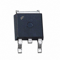
HUFA75429D3ST Fairchild Semiconductor, HUFA75429D3ST Datasheet - Page 5

HUFA75429D3ST
Manufacturer Part Number
HUFA75429D3ST
Description
MOSFET N-CH 60V 20A DPAK
Manufacturer
Fairchild Semiconductor
Series
UltraFET™r
Datasheet
1.HUFA75429D3ST.pdf
(11 pages)
Specifications of HUFA75429D3ST
Fet Type
MOSFET N-Channel, Metal Oxide
Fet Feature
Logic Level Gate
Rds On (max) @ Id, Vgs
25 mOhm @ 20A, 10V
Drain To Source Voltage (vdss)
60V
Current - Continuous Drain (id) @ 25° C
20A
Vgs(th) (max) @ Id
4V @ 250µA
Gate Charge (qg) @ Vgs
85nC @ 20V
Input Capacitance (ciss) @ Vds
1090pF @ 25V
Power - Max
125W
Mounting Type
Surface Mount
Package / Case
DPak, TO-252 (2 leads+tab), SC-63
Configuration
Single
Transistor Polarity
N-Channel
Resistance Drain-source Rds (on)
0.021 Ohms
Drain-source Breakdown Voltage
60 V
Gate-source Breakdown Voltage
+/- 20 V
Continuous Drain Current
20 A
Power Dissipation
125 W
Maximum Operating Temperature
+ 175 C
Mounting Style
SMD/SMT
Fall Time
33 ns
Minimum Operating Temperature
- 55 C
Rise Time
39 ns
Lead Free Status / RoHS Status
Lead free / RoHS Compliant
©2003 Fairchild Semiconductor Corporation
Typical Characteristics
Test Circuits and Waveforms
VARY t
REQUIRED PEAK I
Breakdown Voltage vs Junction Temperature
0V
Figure 14. Unclamped Energy Test Circuit
1.2
1.1
1.0
0.9
Figure 11. Normalized Drain to Source
P
-80
TO OBTAIN
I
V
D
t
GS
P
= 250 A
-40
AS
T
J
, JUNCTION TEMPERATURE (
0
Figure 13. Gate Charge Waveforms for Constant Gate Currents
R
G
40
10
80
8
6
4
2
0
0
T
A
V
V
= 25°C unless otherwise noted
I
AS
120
DS
DD
o
C)
= 30V
DUT
0.01
L
160
10
Q
+
-
g
V
, GATE CHARGE (nC)
DD
200
20
0
3000
1000
WAVEFORMS IN
DESCENDING ORDER:
Figure 12. Capacitance vs Drain to Source
Figure 15. Unclamped Energy Waveforms
100
50
0.1
I
I
D
D
= 20A
= 4A
C
V
30
RSS
GS
= 0V, f = 1MHz
V
DS
C
C
, DRAIN TO SOURCE VOLTAGE (V)
GD
OSS
I
AS
C
t
Voltage
40
DS
1
P
+ C
GD
BV
t
AV
DSS
C
ISS
10
V
C
DS
GS
+ C
GD
V
DD
60
Rev. A1


