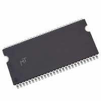
MT48LC16M16A2P-75 L:D TR Micron Technology Inc, MT48LC16M16A2P-75 L:D TR Datasheet - Page 46

MT48LC16M16A2P-75 L:D TR
Manufacturer Part Number
MT48LC16M16A2P-75 L:D TR
Description
DRAM Chip SDRAM 256M-Bit 16Mx16 3.3V 54-Pin TSOP-II T/R
Manufacturer
Micron Technology Inc
Type
SDRAMr
Specifications of MT48LC16M16A2P-75 L:D TR
Package
54TSOP-II
Density
256 Mb
Address Bus Width
15 Bit
Operating Supply Voltage
3.3 V
Maximum Clock Rate
133 MHz
Maximum Random Access Time
6|5.4 ns
Operating Temperature
0 to 70 °C
Format - Memory
RAM
Memory Type
SDRAM
Memory Size
256M (16Mx16)
Speed
133MHz
Interface
Parallel
Voltage - Supply
3 V ~ 3.6 V
Package / Case
54-TSOP II
Lead Free Status / RoHS Status
Lead free / RoHS Compliant
Other names
557-1191-2
- Current page: 46 of 92
- Download datasheet (3Mb)
Mode Register
PDF: 09005aef8091e6d1
256Mb_sdr.pdf - Rev. N 1/10 EN
The mode register defines the specific mode of operation, including burst length (BL),
burst type, CAS latency (CL), operating mode, and write burst mode. The mode register
is programmed via the LOAD MODE REGISTER command and retains the stored infor-
mation until it is programmed again or the device loses power.
Mode register bits M[2:0] specify the BL; M3 specifies the type of burst; M[6:4] specify
the CL; M7 and M8 specify the operating mode; M9 specifies the write burst mode; and
M10–Mn should be set to zero to ensure compatibility with future revisions. Mn + 1 and
Mn + 2 should be set to zero to select the mode register.
The mode registers must be loaded when all banks are idle, and the controller must
wait
ments will result in unspecified operation.
t
MRD before initiating the subsequent operation. Violating either of these require-
46
Micron Technology, Inc. reserves the right to change products or specifications without notice.
256Mb: x4, x8, x16 SDRAM
© 1999 Micron Technology, Inc. All rights reserved.
Mode Register
Related parts for MT48LC16M16A2P-75 L:D TR
Image
Part Number
Description
Manufacturer
Datasheet
Request
R

Part Number:
Description:
DRAM Chip SDRAM 256M-Bit 16Mx16 3.3V 54-Pin TSOP-II Tray
Manufacturer:
Micron Technology Inc
Datasheet:

Part Number:
Description:
DRAM Chip SDRAM 256M-Bit 16Mx16 3.3V 54-Pin TSOP-II Tray
Manufacturer:
Micron Technology Inc
Datasheet:

Part Number:
Description:
IC, SDRAM, 256MBIT, 133MHZ, TSOP-54
Manufacturer:
Micron Technology Inc
Datasheet:

Part Number:
Description:
SDRAM 256MB, SMD, 48LC16, TSOP54
Manufacturer:
Micron Technology Inc
Datasheet:

Part Number:
Description:
Manufacturer:
Micron Technology Inc
Datasheet:

Part Number:
Description:
Manufacturer:
Micron Technology Inc
Datasheet:

Part Number:
Description:
Manufacturer:
Micron Technology Inc
Datasheet:

Part Number:
Description:
IC SDRAM 256MBIT 167MHZ 54TSOP
Manufacturer:
Micron Technology Inc
Datasheet:

Part Number:
Description:
IC SDRAM 256MBIT 133MHZ 54TSOP
Manufacturer:
Micron Technology Inc
Datasheet:

Part Number:
Description:
IC SDRAM 256MBIT 133MHZ 54TSOP
Manufacturer:
Micron Technology Inc
Datasheet:

Part Number:
Description:
IC SDRAM 256MBIT 133MHZ 54TSOP
Manufacturer:
Micron Technology Inc
Datasheet:

Part Number:
Description:
DRAM Chip SDRAM 256M-Bit 16Mx16 3.3V 54-Pin TSOP-II T/R
Manufacturer:
Micron Technology Inc
Datasheet:

Part Number:
Description:
DRAM Chip SDRAM 256M-Bit 16Mx16 3.3V 54-Pin TSOP-II Tray
Manufacturer:
Micron Technology Inc
Datasheet:

Part Number:
Description:
DRAM Chip SDRAM 256M-Bit 16Mx16 3.3V 54-Pin TSOP-II T/R
Manufacturer:
Micron Technology Inc
Datasheet:

Part Number:
Description:
DRAM Chip SDRAM 256M-Bit 16Mx16 3.3V 54-Pin TSOP-II Tray
Manufacturer:
Micron Technology Inc
Datasheet:


