XA3S500E-4PQG208Q Xilinx Inc, XA3S500E-4PQG208Q Datasheet - Page 14
XA3S500E-4PQG208Q
Manufacturer Part Number
XA3S500E-4PQG208Q
Description
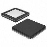
FPGA XA Spartan™-3E Family 500K Gates 10476 Cells 572MHz 90nm Technology 1.2V 208-Pin PQFP
Manufacturer
Xilinx Inc
Series
Spartan™-3E XAr
Datasheet
1.XA3S100E-4VQG100I.pdf
(37 pages)
Specifications of XA3S500E-4PQG208Q
Package
208PQFP
Family Name
XA SpartanÂ-3E
Device Logic Units
10476
Device System Gates
500000
Maximum Internal Frequency
572 MHz
Typical Operating Supply Voltage
1.2 V
Maximum Number Of User I/os
158
Ram Bits
368640
Number Of Logic Elements/cells
10476
Number Of Labs/clbs
1164
Total Ram Bits
368640
Number Of I /o
158
Number Of Gates
500000
Voltage - Supply
1.14 V ~ 1.26 V
Mounting Type
Surface Mount
Operating Temperature
-40°C ~ 125°C
Package / Case
208-BFQFP
Lead Free Status / RoHS Status
Lead free / RoHS Compliant
Available stocks
Company
Part Number
Manufacturer
Quantity
Price
Company:

Part Number:
XA3S500E-4PQG208Q
Manufacturer:
Xilinx Inc
Quantity:
10 000
Part Number:
XA3S500E-4PQG208Q
Manufacturer:
XILINX/赛灵思
Quantity:
20 000


Switching Characteristics
I/O Timing
Table 13: Pin-to-Pin Clock-to-Output Times for the IOB Output Path
DS635 (v2.0) September 9, 2009
Product Specification
Notes:
1.
2.
3.
4.
Clock-to-Output Times
T
The numbers in this table are tested using the methodology presented in
Table 6
This clock-to-output time requires adjustment whenever a signal standard other than LVCMOS25 is assigned to the Global Clock Input or a
standard other than LVCMOS25 with 12 mA drive and Fast slew rate is assigned to the data Output. If the former is true, add the appropriate
Input adjustment from
DCM output jitter is included in all measurements.
For minimums, use the values reported by the Xilinx timing analyzer.
Symbol
ICKOFDCM
T
ICKOF
and
R
Table
Figure 5: External Termination Resistors for BLVDS Transmitter and BLVDS Receiver
When reading from the Output
Flip-Flop (OFF), the time from
the active transition on the
Global Clock pin to data
appearing at the Output pin. The
DCM is used.
When reading from OFF, the
time from the active transition on
the Global Clock pin to data
appearing at the Output pin. The
DCM is not used.
9.
Table
17. If the latter is true, add the appropriate Output adjustment from
V
Description
CCO
= 2.5V
165Ω
165Ω
1/4th of Bourns
CAT16-LV4F12
Part Number
140Ω
LVCMOS25
output drive, Fast slew rate,
with DCM
LVCMOS25
output drive, Fast slew rate,
without DCM
www.xilinx.com
Z
Z
Conditions
0
0
(3)
= 50Ω
= 50Ω
(2)
(2)
Table 19
, 12mA
, 12mA
1/4th of Bourns
CAT16-PT4F4
Part Number
and are based on the operating conditions set forth in
100Ω
V
XA3S100E
XA3S250E
XA3S500E
XA3S1200E
XA3S1600E
XA3S100E
XA3S250E
XA3S500E
XA3S1200E
XA3S1600E
DS635_05_082807
CCO
Table
Device
= 2.5V
18.
-4 Speed
Grade
Max
2.79
3.45
3.46
3.46
3.45
5.92
5.43
5.51
5.94
6.05
Units
ns
ns
ns
ns
ns
ns
ns
ns
ns
ns
14
Related parts for XA3S500E-4PQG208Q
Image
Part Number
Description
Manufacturer
Datasheet
Request
R

Part Number:
Description:
IC FPGA SPARTAN-3E 500K 256FTBGA
Manufacturer:
Xilinx Inc
Datasheet:

Part Number:
Description:
IC FPGA SPARTAN-3E 256FPBGA
Manufacturer:
Xilinx Inc
Datasheet:

Part Number:
Description:
IC FPGA SPARTAN-3E 500K 132CSBGA
Manufacturer:
Xilinx Inc
Datasheet:
Part Number:
Description:
IC FPGA SPARTAN-3E 500K 132CSBGA
Manufacturer:
Xilinx Inc
Datasheet:

Part Number:
Description:
IC FPGA SPARTAN-3E 500K 208-PQFP
Manufacturer:
Xilinx Inc
Datasheet:
Part Number:
Description:
IC FPGA SPARTAN-3E 500K 256FTBGA
Manufacturer:
Xilinx Inc
Datasheet:

Part Number:
Description:
IC CPLD .8K 36MCELL 44-VQFP
Manufacturer:
Xilinx Inc
Datasheet:

Part Number:
Description:
IC CPLD 72MCRCELL 10NS 44VQFP
Manufacturer:
Xilinx Inc
Datasheet:

Part Number:
Description:
IC CPLD 1.6K 72MCELL 64-VQFP
Manufacturer:
Xilinx Inc
Datasheet:

Part Number:
Description:
IC CR-II CPLD 64MCELL 44-VQFP
Manufacturer:
Xilinx Inc
Datasheet:

Part Number:
Description:
IC CPLD 1.6K 72MCELL 100-TQFP
Manufacturer:
Xilinx Inc
Datasheet:

Part Number:
Description:
IC CR-II CPLD 64MCELL 56-BGA
Manufacturer:
Xilinx Inc
Datasheet:

Part Number:
Description:
IC CPLD 72MCRCELL 7.5NS 44VQFP
Manufacturer:
Xilinx Inc
Datasheet:
Part Number:
Description:
IC CR-II CPLD 64MCELL 100-VQFP
Manufacturer:
Xilinx Inc
Datasheet:
Part Number:
Description:
IC CPLD 1.6K 72MCELL 100-TQFP
Manufacturer:
Xilinx Inc
Datasheet: