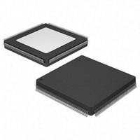
XA3S500E-4PQG208Q Xilinx Inc, XA3S500E-4PQG208Q Datasheet - Page 22

XA3S500E-4PQG208Q
Manufacturer Part Number
XA3S500E-4PQG208Q
Description
FPGA XA Spartan™-3E Family 500K Gates 10476 Cells 572MHz 90nm Technology 1.2V 208-Pin PQFP
Manufacturer
Xilinx Inc
Series
Spartan™-3E XAr
Datasheet
1.XA3S100E-4VQG100I.pdf
(37 pages)
Specifications of XA3S500E-4PQG208Q
Package
208PQFP
Family Name
XA SpartanÂ-3E
Device Logic Units
10476
Device System Gates
500000
Maximum Internal Frequency
572 MHz
Typical Operating Supply Voltage
1.2 V
Maximum Number Of User I/os
158
Ram Bits
368640
Number Of Logic Elements/cells
10476
Number Of Labs/clbs
1164
Total Ram Bits
368640
Number Of I /o
158
Number Of Gates
500000
Voltage - Supply
1.14 V ~ 1.26 V
Mounting Type
Surface Mount
Operating Temperature
-40°C ~ 125°C
Package / Case
208-BFQFP
Lead Free Status / RoHS Status
Lead free / RoHS Compliant
Available stocks
Company
Part Number
Manufacturer
Quantity
Price
Company:
Part Number:
XA3S500E-4PQG208Q
Manufacturer:
Xilinx Inc
Quantity:
10 000
Part Number:
XA3S500E-4PQG208Q
Manufacturer:
XILINX/赛灵思
Quantity:
20 000
Clock Buffer/Multiplexer Switching Characteristics
Table 23: Clock Distribution Switching Characteristics
18 x 18 Embedded Multiplier Timing
Table 24: 18 x 18 Embedded Multiplier Timing
DS635 (v2.0) September 9, 2009
Product Specification
Global clock buffer (BUFG, BUFGMUX, BUFGCE) I input to O-output
delay
Global clock multiplexer (BUFGMUX) select S-input setup to I0 and I1
inputs. Same as BUFGCE enable CE-input
Frequency of signals distributed on global buffers (all sides)
Combinatorial Delay
T
Clock-to-Output Times
T
T
T
Setup Times
T
T
T
Hold Times
T
T
T
MULT
MSCKP_P
MSCKP_A
MSCKP_B
MSDCK_P
MSDCK_A
MSDCK_B
MSCKD_P
MSCKD_A
MSCKD_B
Symbol
R
Combinatorial multiplier propagation delay from the A and B inputs to
the P outputs, assuming 18-bit inputs and a 36-bit product (AREG,
BREG, and PREG registers unused)
Clock-to-output delay from the active transition of the CLK input to valid
data appearing on the P outputs when using the PREG register
Clock-to-output delay from the active transition of the CLK input to valid
data appearing on the P outputs when using either the AREG or BREG
register
Data setup time at the A or B input before the active transition at the
CLK when using only the PREG output register (AREG, BREG
registers unused)
Data setup time at the A input before the active transition at the CLK
when using the AREG input register
Data setup time at the B input before the active transition at the CLK
when using the BREG input register
Data hold time at the A or B input before the active transition at the CLK
when using only the PREG output register (AREG, BREG registers
unused)
Data hold time at the A input before the active transition at the CLK
when using the AREG input register
Data hold time at the B input before the active transition at the CLK
when using the BREG input register
(3)
(2)
Description
(2)
Description
www.xilinx.com
(3)
(3)
(3)
(3)
Symbol
F
T
T
BUFG
GIO
GSI
(2)
-4 Speed Grade
Maximum
-4 Speed Grade
-0.97
3.98
0.23
0.39
0.04
0.05
Min
-
-
-
1.46
0.63
311
4.88
Max
1.10
4.97
-
-
-
(1)
Units
MHz
ns
ns
Units
ns
ns
ns
ns
ns
ns
22


