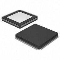
XA3S500E-4PQG208Q Xilinx Inc, XA3S500E-4PQG208Q Datasheet - Page 35

XA3S500E-4PQG208Q
Manufacturer Part Number
XA3S500E-4PQG208Q
Description
FPGA XA Spartan™-3E Family 500K Gates 10476 Cells 572MHz 90nm Technology 1.2V 208-Pin PQFP
Manufacturer
Xilinx Inc
Series
Spartan™-3E XAr
Datasheet
1.XA3S100E-4VQG100I.pdf
(37 pages)
Specifications of XA3S500E-4PQG208Q
Package
208PQFP
Family Name
XA SpartanÂ-3E
Device Logic Units
10476
Device System Gates
500000
Maximum Internal Frequency
572 MHz
Typical Operating Supply Voltage
1.2 V
Maximum Number Of User I/os
158
Ram Bits
368640
Number Of Logic Elements/cells
10476
Number Of Labs/clbs
1164
Total Ram Bits
368640
Number Of I /o
158
Number Of Gates
500000
Voltage - Supply
1.14 V ~ 1.26 V
Mounting Type
Surface Mount
Operating Temperature
-40°C ~ 125°C
Package / Case
208-BFQFP
Lead Free Status / RoHS Status
Lead free / RoHS Compliant
Available stocks
Company
Part Number
Manufacturer
Quantity
Price
Company:
Part Number:
XA3S500E-4PQG208Q
Manufacturer:
Xilinx Inc
Quantity:
10 000
Part Number:
XA3S500E-4PQG208Q
Manufacturer:
XILINX/赛灵思
Quantity:
20 000
IEEE 1149.1/1553 JTAG Test Access Port Timing
Table 44: Timing for the JTAG Test Access Port
DS635 (v2.0) September 9, 2009
Product Specification
Notes:
1.
Clock-to-Output Times
T
Setup Times
T
T
Hold Times
T
T
Clock Timing
T
T
F
TCKTDO
TDITCK
TMSTCK
TCKTDI
TCKTMS
CCH
CCL
TCK
The numbers in this table are based on the operating conditions set forth in
Symbol
R
The time from the falling transition on the TCK pin
to data appearing at the TDO pin
The time from the setup of data at the TDI pin to
the rising transition at the TCK pin
The time from the setup of a logic level at the TMS
pin to the rising transition at the TCK pin
The time from the rising transition at the TCK pin
to the point when data is last held at the TDI pin
The time from the rising transition at the TCK pin
to the point when a logic level is last held at the
TMS pin
The High pulse width at the TCK pin
The Low pulse width at the TCK pin
Frequency of the TCK signal
Description
www.xilinx.com
Table
6.
Min
1.0
7.0
7.0
0
0
5
5
-
-4 Speed Grade
Max
11.0
25
-
-
-
-
-
-
Units
MHz
ns
ns
ns
ns
ns
ns
ns
35


