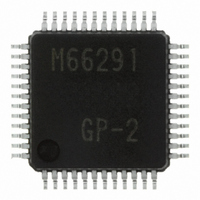
M66291GP#201 Renesas Electronics America, M66291GP#201 Datasheet - Page 20

M66291GP#201
Manufacturer Part Number
M66291GP#201
Description
IC USB CONTROLLER GEN-PUR 48LQFP
Manufacturer
Renesas Electronics America
Datasheet
1.M66291GP201.pdf
(126 pages)
Specifications of M66291GP#201
Package / Case
48-LQFP
Mounting Type
Surface Mount
Current - Supply
30mA
Voltage - Supply
3 V ~ 3.6 V
Operating Temperature
-20°C ~ 85°C
Interface
Serial
Controller Type
USB 2.0 Controller
Lead Free Status / RoHS Status
Not Compliant
Available stocks
Company
Part Number
Manufacturer
Quantity
Price
M 6 6 2 9 1 G P / H P
R e v 1 . 0 1
(6) BE01 (Buffer Empty/Size Over Error Interrupt Assign) Bit (b10)
(7) NR01 (Buffer Not Ready Interrupt Assign) Bit (b9)
(8) RD01 (Buffer Ready Interrupt Assign) Bit (b8)
(9) RDYM (Buffer Ready Mode) Bit (b2)
(10) INTL (Interrupt Output Sense) Bit (b1)
Note :
Note : SCKE bit = “0” when XCKE bit = “1 ” , or XCKE bit = “0”.
This bit selects the pin to output the buffer empty/size over error interrupt signal.
This bit selects the pin to output the buffer not ready interrupt signal.
This bit selects the pin to output the buffer ready interrupt signal.
This bit selects the method of clearing the buffer ready interrupt.
When this bit is set to “0”, the EPB_RDY bit is cleared to “0” after the CPU side buffer data are all read out or
after the writing of transmit data completes.
When this bit is set to “1”, the EPB_RDY bit is cleared to “0” by writing “0” to the EPB_RDY bit.
For details, refer to “EPB_RDY bit”.
This bit sets the sense mode for interrupt output from INT0 or INT1 pin.
When this bit is set to “0”, the INT0 or INT1 pin notifies the occurrence of interrupt at the edge set by the
INTA bit.
During edge sensitive output, when “0” is written to each interrupt factor bit to clear the interrupt, the output
signal outputs the negate value one time. If the other interrupt factor bits are set to “1”, the occurrence of
interrupt again is notified at the edge. The negate period is equivalent to 32 clocks (approx. 667 ns) of the 48
MHz clock.
In case the clock is not supplied (Note), the negate period does not occur. Make sure not to miss the interrupt
when Vbus interrupt or resume interrupt occurs.
When this bit is set to “1”, the INT0 or INT1 pin notifies the occurrence of interrupt at the level set by the
INTA bit.
During level sensitive output, the negate fails to work unless all interrupt factor bits are cleared even if “0” is
written to clear the interrupt to the interrupt factor bits.
Refer to Figure 2.5 and “3.1 Interrupt Function”.
2 0 0 4 . 1 1 . 0 1
Refer to “3.2 FIFO Buffer” for CPU/SIE side.
p a g e 2 0 o f 1 2 2


