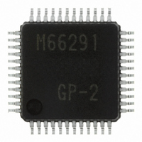
M66291GP#201 Renesas Electronics America, M66291GP#201 Datasheet - Page 66

M66291GP#201
Manufacturer Part Number
M66291GP#201
Description
IC USB CONTROLLER GEN-PUR 48LQFP
Manufacturer
Renesas Electronics America
Datasheet
1.M66291GP201.pdf
(126 pages)
Specifications of M66291GP#201
Package / Case
48-LQFP
Mounting Type
Surface Mount
Current - Supply
30mA
Voltage - Supply
3 V ~ 3.6 V
Operating Temperature
-20°C ~ 85°C
Interface
Serial
Controller Type
USB 2.0 Controller
Lead Free Status / RoHS Status
Not Compliant
Available stocks
Company
Part Number
Manufacturer
Quantity
Price
M 6 6 2 9 1 G P / H P
R e v 1 . 0 1
(9) Octl (Register 8-Bit Mode) Bit (b6)
(10) DMA_EP (DMA Transfer Endpoint Designate) Bits (b3~b0)
This bit sets the access mode of the Dn_FIFO Data Register.
When this bit is set to “0”, the Dn_FIFO Data Register is set to 16-bit mode, and all bits of the Dn_FIFO Data
Register are valid.
When this bit is set to “1”, the Dn_FIFO Data Register is set to 8-bit mode, and the upper-order 8 bits of the
Dn_FIFO Data Register (b15 to b8) are invalid.
When set to OUT buffer (EPi_DIR bit = “0”), change this bit before receiving the data. When set to IN buffer
(EPi_DIR bit = “1”), if the Dreq bit is equal to “1”, do not change this bit.
This bit becomes invalid (fixed to 8-bit mode) when the mode is set to 8-bit by *HWR/*BYTE pin.
In such case, this bit is read “0”.
These bits select the endpoint of DMA transfer.
Make sure that the endpoint selection does not get overlapped with the selection by the CPU_EP bits.
When making a change in these bits to select the other endpoint, make sure that the source endpoint and the
destination endpoint to be changed are not under the access by the CPU/DMA or during
receiving/transmitting of SIE (under access to FIFO buffer).
2 0 0 4 . 1 1 . 0 1
Note:
Note:
The access width of the Dn_FIFO Data Register is controlled by the logical sum of this bit and the EPi_Octl bits
of the EPi Configuration Register 1 specified by the DMA_EP bits. Hence, the mode is set to 8-bit if “1” is set to
either this bit or to the EPi_Octl bits of the EPi Configuration Register 1. Make sure that both bits must be set to
“0” to change to 16-bit mode.
Do not change this bit while accessing the Dn_FIFO Data Register.
p a g e 6 6 o f 1 2 2


