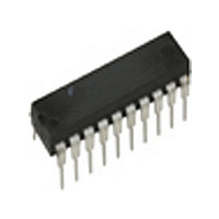
ML4819CP_NL Fairchild Semiconductor, ML4819CP_NL Datasheet - Page 7

ML4819CP_NL
Manufacturer Part Number
ML4819CP_NL
Description
Manufacturer
Fairchild Semiconductor
Datasheet
1.ML4819CP_NL.pdf
(15 pages)
Specifications of ML4819CP_NL
Start-up Supply Current
600uA
Operating Supply Voltage (max)
35V
Operating Temp Range
0C to 70C
Operating Temperature Classification
Commercial
Package Type
PDIP
Pin Count
20
Mounting
Through Hole
Lead Free Status / RoHS Status
Compliant
SLOPE COMPENSATION
Slope compensation is accomplished by adding 1/2 of the
current flowing out of pin 12 to pin 1 (for the PFC section
and pin 9 (for the PWM section). The amount of slope
compensation is equal to (I
the impedance to GND on pin 1 or pin 9. Since most of
the PWM applications will be limited to 50% duty cycle,
slope compensation should not be needed for the PWM
section. This can be defeated by using a low impedance
load to the current sense on pin 9.
UNDER VOLTAGE LOCKOUT
On power-up the ML4819 remains in the UVLO condition;
output low and quiescent current low. The IC becomes
operational when V
below 10V, the UVLO condition is imposed. During the
UVLO condition, the 5V V
usable as a status flag.
REV. 1.0 10/10/2000
500
400
300
200
100
0
R
0
SC
RAMP COMP
12
10
20
Figure 7. Slope Compensation Circuit
Figure 8. Gain Modulator Linearity
R
C
T
T
100
SINE INPUT CURRENT (µA)
CC
I
R(SC)
Q1
reaches 16V. When V
V
COMPENSATION
200
REF
SLOPE
REF
RAMP COMP
OSC
pin is “off”, making it
9V
300
I
I
R(SC)
R(SC)
/2)
2
2
400
R
CC
L
where R
drops
TO PIN 9
TO PIN 1
500
1. 5V
4.5V
4.0V
3.5V
3.0V
2.5V
2.0V
L
is
40
30
20
10
Figure 10a. Total Supply Current vs. Supply Voltage
0
Figure 10b. Supply Current (I
Figure 9. Under-Voltage Lockout Block Diagram
0
35
30
25
20
15
10
5
0
0
GEN.
10
V
10
REF
+
–
ENABLE
V
9V
20
V
CC,
REF
TEMPERATURE ( C)
SUPPLY VOLTAGE (V)
30
INTERNAL
OPERATING
START-UP
CURRENT
20
BIAS
40
CC
) vs. Temperature
50
T
A
= 25 C
30
60
ML4819
5V V
V
CC
70
REF
40
7


