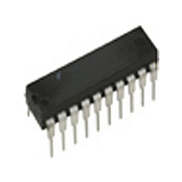
ML4819CP_NL Fairchild Semiconductor, ML4819CP_NL Datasheet - Page 8

ML4819CP_NL
Manufacturer Part Number
ML4819CP_NL
Description
Manufacturer
Fairchild Semiconductor
Datasheet
1.ML4819CP_NL.pdf
(15 pages)
Specifications of ML4819CP_NL
Start-up Supply Current
600uA
Operating Supply Voltage (max)
35V
Operating Temp Range
0C to 70C
Operating Temperature Classification
Commercial
Package Type
PDIP
Pin Count
20
Mounting
Through Hole
Lead Free Status / RoHS Status
Compliant
ML4819
APPLICATIONS
POWER FACTOR SECTION
The power factor section in the ML4819 is similar to the
power factor section in the ML4812 with the exception of
the operation of the slope compensation circuit. Please
refer to the ML4812 data sheet for more information.
The following calculations refer to Figure 12 in this data
sheet. The component designators in the equations below
refer to the following components in Figure 12:
INPUT INDUCTOR (L1) SELECTION
The central component in the regulator is the input boost
inductor. The value of this inductor controls various
critical operational aspects of the regulator. If the value is
too low, the input current distortion will be high and will
result in low power factor and increased noise at the
input. This will require more input filtering. In addition,
when the value of the inductor is low the inductor dries
out (runs out of current) at low currents. Thus the power
factor will decrease at lower power levels and/or higher
line voltages. If the inductor value is too high, then for a
given operating current the required size of the inductor
core will be large and/or the required number of turns will
be high. So a balance must be reached between distortion
and core size.
One more condition where the inductor can dry out is
analyzed below where it is shown to be maximum duty
cycle dependent.
For the boost converter at steady state:
8
–4.0
–8.0
–12
–16
–20
–24
0
R
V
0
T
OUT
= R16, C
Figure 11. Reference Load Regulation
1
20
V
D
I
T
IN
REF
ON
= C6.
, REFERENCE SOURCE CURRENT (mA)
40
60
80
T
A
= 25 C
V
100
CC
= 15V
(1)
120
Where D
input boost inductor will dry out when the following
condition is satisfied:
or
V
V
Effectively, the above relationship shows that the resetting
volt-seconds are more than setting volt-seconds. In energy
transfer terms this means that less energy is stored in the
inductor during the ON time than it is asked to deliver during
the OFF time. The net result is that the inductor dries out.
The recommended maximum duty cycle is 95% at
100KHz to allow time for the input inductor to dump its
energy to the output capacitors.
For example:
if: V
then substituting in (3) yields V
drying out is an increase in distortion at low input voltages.
For a given output power, the instantaneous value of the
input current is a function of the input sinusoidal voltage
waveform. As the input voltage sweeps from zero volts to
its maximum value and back, so does the current.
The load of the power factor regulator is usually a
switching power supply which is essentially a constant
power load. As a result, an increase in the input voltage
will be offset by a decrease in the input current.
By combining the ideas set forth above, some ground
rules can be obtained for the selection and design of the
input inductor:
Step 1: Find minimum operating current.
then:
Step 2: Choose a minimum current at which point the
INDRY
OUT
D
V
P
I
V
I
IN(MIN)PEAK
IN MIN PEAK
: Output dc voltage.
IN(MIN)
OUT
IN(MAX)
INDRY
ON(MAX)
V t
(
: Voltage where the inductor dries out.
IN
inductor current will be on the verge of drying
out. For this example 40% of the peak current
found in step 1 was chosen.
ON
( )
= 380V and
)
is the duty cycle [T
= 50W
= 260V
V
1
= 0.95
OUT
= 0.272A
D
. 1 414
ON MAX
V
1
(
IN MAX
(
D
P
)
ON MAX
IN MIN
(
)
(
V
INDRY
OUT
ON
)
)
/(T
= 20V. The effect of
ON
REV. 1.0 10/10/2000
+ T
OFF
)]. The
(2)
(3)
(4)


