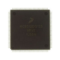
MC9S12DG128VPVE Freescale, MC9S12DG128VPVE Datasheet - Page 3

MC9S12DG128VPVE
Manufacturer Part Number
MC9S12DG128VPVE
Description
Manufacturer
Freescale
Datasheet
1.MC9S12DG128VPVE.pdf
(142 pages)
Specifications of MC9S12DG128VPVE
Cpu Family
HCS12
Device Core Size
16b
Frequency (max)
50MHz
Interface Type
SCI/SPI/I2C/CAN
Total Internal Ram Size
8KB
# I/os (max)
91
Number Of Timers - General Purpose
8
Operating Supply Voltage (typ)
2.5/5V
Operating Supply Voltage (max)
2.75/5.25V
Operating Supply Voltage (min)
2.25/2.35/4.5V
On-chip Adc
2(8-chx10-bit)
Instruction Set Architecture
CISC
Operating Temp Range
-40C to 105C
Operating Temperature Classification
Industrial
Mounting
Surface Mount
Pin Count
112
Package Type
LQFP
Program Memory Type
Flash
Program Memory Size
128KB
Lead Free Status / RoHS Status
Compliant
Available stocks
Company
Part Number
Manufacturer
Quantity
Price
Company:
Part Number:
MC9S12DG128VPVE
Manufacturer:
Freescale Semiconductor
Quantity:
10 000
Freescale Semiconductor
Number
Version
V02.02
V02.03
V02.04
V02.05
V02.06
Revision
08 Mar
14 Mar
16 Aug
12 Sep
06 Nov
Date
2002
2002
2002
2002
2002
Effective
12 Sep
08 Mar
14 Mar
16 Aug
06 Nov
Date
2002
2002
2002
2002
2002
Author
Changed XCLKS to PE7 in Table 2-2
Updated device part numbers in Figure 2-1
Updated BDM clock in Figure 3-1
Removed SIM description in overview & n
Updated electrical spec of VDD & VDDPLL (Table A-4), IOL/IOH
(Table A-6), C
Updated interrupt pulse timing variables in Table A-6
Updated device part numbers in Figure 2-1
Added document numbers on cover page and Table 0-2
Cleaned up Fig. 1-1, 2-1
Updated Section 1.5 descriptions
Corrected PE assignment in Table 2-2, Fig. 2-5,6,7.
Corrected NVM sizes in Sections 16, 17
Added I
Added Blank Check in A.3.1.5 and Table A-11
Updated CRG spec in Table A-15
Added:
Pull-up columns to signal table,
Example for PLL Filter calculation,
Thermal values for junction to board and package,
BGND pin pull-up
Part Order Information
Global Register Table
Chip Configuration Summary
Device specific info on CRG
Modified:
Reduced Wait and Run IDD values
Mode of Operation chapter
Changed leakage current for ADC inputs down to +-1uA
Minor modification of PLL frequency/ voltage gain values
Corrected:
Pin names/functions on 80 pin packages
Interrupt vector table enable register inconsistencies
PCB layout for 80QFP VREGEN position
Corrected:
Register address mismatches in 1.5.1
Removed document order no. from Revision History pages
Renamed "Preface" section to "Derivative Differences and
Document references". Added details for derivatives missing
CAN0/1/4, BDLC, IIC and/or Byteflight
Added 2L40K mask set in section 1.6
Added OSC User Guide in Preface, “Document References”
Added oscillator clock connection to BDM in S12_CORE in fig 3-1
Corrected several register and bit names in “Local Enable” column
of Table 5.1 Interrupt Vector Locations
Section HCS12 Core Block Description: mentioned alternate clock
of BDM to be equivalent to oscillator clock
Added new section: “Oscillator (OSC) Block Description”
Corrected in footnote of Table "PLL Characteristics": fOSC = 4MHz
REF
spec for 1ATD in Table A-8
INS
Device User Guide — 9S12DT128DGV2/D V02.16
(Table A-9), C
Description of Changes
IN
(Table A-6 & A-15),
UPOSC
spec in Table A-15
3


