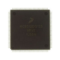
MC9S12DG128VPVE Freescale, MC9S12DG128VPVE Datasheet - Page 98

MC9S12DG128VPVE
Manufacturer Part Number
MC9S12DG128VPVE
Description
Manufacturer
Freescale
Datasheet
1.MC9S12DG128VPVE.pdf
(142 pages)
Specifications of MC9S12DG128VPVE
Cpu Family
HCS12
Device Core Size
16b
Frequency (max)
50MHz
Interface Type
SCI/SPI/I2C/CAN
Total Internal Ram Size
8KB
# I/os (max)
91
Number Of Timers - General Purpose
8
Operating Supply Voltage (typ)
2.5/5V
Operating Supply Voltage (max)
2.75/5.25V
Operating Supply Voltage (min)
2.25/2.35/4.5V
On-chip Adc
2(8-chx10-bit)
Instruction Set Architecture
CISC
Operating Temp Range
-40C to 105C
Operating Temperature Classification
Industrial
Mounting
Surface Mount
Pin Count
112
Package Type
LQFP
Program Memory Type
Flash
Program Memory Size
128KB
Lead Free Status / RoHS Status
Compliant
Available stocks
Company
Part Number
Manufacturer
Quantity
Price
Company:
Part Number:
MC9S12DG128VPVE
Manufacturer:
Freescale Semiconductor
Quantity:
10 000
Device User Guide — 9S12DT128DGV2/D V02.16
A.1.3 Pins
There are four groups of functional pins.
A.1.3.1 5V I/O pins
Those I/O pins have a nominal level of 5V. This class of pins is comprised of all port I/O pins, the analog
inputs, BKGD pin and the RESET inputs.The internal structure of all those pins is identical, however some
of the functionality may be disabled. E.g. for the analog inputs the output drivers, pull-up and pull-down
resistors are disabled permanently.
A.1.3.2 Analog Reference
This class is made up by the two VRH and VRL pins.
A.1.3.3 Oscillator
The pins XFC, EXTAL, XTAL dedicated to the oscillator have a nominal 2.5V level. They are supplied
by VDDPLL.
A.1.3.4 TEST
This pin is used for production testing only.
A.1.3.5 VREGEN
This pin is used to enable the on chip voltage regulator.
A.1.4 Current Injection
Power supply must maintain regulation within operating V
operating maximum current conditions. If positive injection current (V
injection current may flow out of VDD5 and could result in external power supply going out of regulation.
Insure external VDD5 load will shunt current greater than maximum injection current. This will be the
greatest risk when the MCU is not consuming power; e.g. if no system clock is present, or if clock rate is
very low which would reduce overall power consumption.
98
NOTE:
In the following context VDD5 is used for either VDDA, VDDR and VDDX; VSS5
is used for either VSSA, VSSR and VSSX unless otherwise noted.
IDD5 denotes the sum of the currents flowing into the VDDA, VDDX and VDDR
pins.
VDD is used for VDD1, VDD2 and VDDPLL, VSS is used for VSS1, VSS2 and
VSSPLL.
IDD is used for the sum of the currents flowing into VDD1 and VDD2.
DD5
or V
DD
in
range during instantaneous and
> V
DD5
Freescale Semiconductor
) is greater than I
DD5
, the


