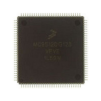
MC9S12DG128VPVE Freescale, MC9S12DG128VPVE Datasheet - Page 73

MC9S12DG128VPVE
Manufacturer Part Number
MC9S12DG128VPVE
Description
Manufacturer
Freescale
Datasheet
1.MC9S12DG128VPVE.pdf
(142 pages)
Specifications of MC9S12DG128VPVE
Cpu Family
HCS12
Device Core Size
16b
Frequency (max)
50MHz
Interface Type
SCI/SPI/I2C/CAN
Total Internal Ram Size
8KB
# I/os (max)
91
Number Of Timers - General Purpose
8
Operating Supply Voltage (typ)
2.5/5V
Operating Supply Voltage (max)
2.75/5.25V
Operating Supply Voltage (min)
2.25/2.35/4.5V
On-chip Adc
2(8-chx10-bit)
Instruction Set Architecture
CISC
Operating Temp Range
-40C to 105C
Operating Temperature Classification
Industrial
Mounting
Surface Mount
Pin Count
112
Package Type
LQFP
Program Memory Type
Flash
Program Memory Size
128KB
Lead Free Status / RoHS Status
Compliant
Available stocks
Company
Part Number
Manufacturer
Quantity
Price
Company:
Part Number:
MC9S12DG128VPVE
Manufacturer:
Freescale Semiconductor
Quantity:
10 000
2.4.1 VDDX,VSSX — Power & Ground Pins for I/O Drivers
External power and ground for I/O drivers. Because fast signal transitions place high, short-duration
current demands on the power supply, use bypass capacitors with high-frequency characteristics and place
them as close to the MCU as possible. Bypass requirements depend on how heavily the MCU pins are
loaded.
2.4.2 VDDR, VSSR — Power & Ground Pins for I/O Drivers & for Internal
Voltage Regulator
transitions place high, short-duration current demands on the power supply, use bypass capacitors with
high-frequency characteristics and place them as close to the MCU as possible. Bypass requirements
depend on how heavily the MCU pins are loaded.
2.4.3 VDD1, VDD2, VSS1, VSS2 — Internal Logic Power Supply Pins
Power is supplied to the MCU through VDD and VSS. Because fast signal transitions place high,
short-duration current demands on the power supply, use bypass capacitors with high-frequency
characteristics and place them as close to the MCU as possible. This 2.5V supply is derived from the
internal voltage regulator. There is no static load on those pins allowed. The internal voltage regulator is
turned off, if VREGEN is tied to ground.
Freescale Semiconductor
External power and ground for I/O drivers and input to the internal voltage regulator. Because fast signal
NOTE:
NOTE:
Mnemonic
VREGEN
VDDPLL
VSSPLL
VDDR
VSSR
VDDX
VDDA
VSSX
VSSA
VRH
VRL
All VSS pins must be connected together in the application.
No load allowed except for bypass capacitors.
112-pin QFP
Pin Number
107
106
41
40
83
86
85
84
43
45
97
Nominal
Voltage
5.0V
5.0V
5.0V
5.0V
2.5V
0V
0V
0V
0V
0V
5V
External power and ground, supply to pin drivers and internal
External power and ground, supply to pin drivers.
Operating voltage and ground for the analog-to-digital
Reference voltages for the analog-to-digital converter.
Provides operating voltage and ground for the Phased-Locked
Internal Voltage Regulator enable/disable
voltage regulator.
converters and the reference for the internal voltage regulator,
allows the supply voltage to the A/D to be bypassed
independently.
Loop. This allows the supply voltage to the PLL to be
bypassed independently. Internal power and ground
generated by internal regulator.
Device User Guide — 9S12DT128DGV2/D V02.16
Description
73


