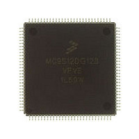
MC9S12DG128VPVE Freescale, MC9S12DG128VPVE Datasheet - Page 89

MC9S12DG128VPVE
Manufacturer Part Number
MC9S12DG128VPVE
Description
Manufacturer
Freescale
Datasheet
1.MC9S12DG128VPVE.pdf
(142 pages)
Specifications of MC9S12DG128VPVE
Cpu Family
HCS12
Device Core Size
16b
Frequency (max)
50MHz
Interface Type
SCI/SPI/I2C/CAN
Total Internal Ram Size
8KB
# I/os (max)
91
Number Of Timers - General Purpose
8
Operating Supply Voltage (typ)
2.5/5V
Operating Supply Voltage (max)
2.75/5.25V
Operating Supply Voltage (min)
2.25/2.35/4.5V
On-chip Adc
2(8-chx10-bit)
Instruction Set Architecture
CISC
Operating Temp Range
-40C to 105C
Operating Temperature Classification
Industrial
Mounting
Surface Mount
Pin Count
112
Package Type
LQFP
Program Memory Type
Flash
Program Memory Size
128KB
Lead Free Status / RoHS Status
Compliant
Available stocks
Company
Part Number
Manufacturer
Quantity
Price
Company:
Part Number:
MC9S12DG128VPVE
Manufacturer:
Freescale Semiconductor
Quantity:
10 000
Section 23 Printed Circuit Board Layout Proposal
The PCB must be carefully laid out to ensure proper operation of the voltage regulator as well as of the
MCU itself. The following rules must be observed:
Freescale Semiconductor
•
•
•
•
•
•
•
Every supply pair must be decoupled by a ceramic capacitor connected as near as possible to the
corresponding pins (C1 – C6).
Central point of the ground star should be the VSSR pin.
Use low ohmic low inductance connections between VSS1, VSS2 and VSSR.
VSSPLL must be directly connected to VSSR.
Keep traces of VSSPLL, EXTAL and XTAL as short as possible and occupied board area for C7,
C8, C11 and Q1 as small as possible.
Do not place other signals or supplies underneath area occupied by C7, C8, C10 and Q1 and the
connection area to the MCU.
Central power input should be fed in at the VDDA/VSSA pins.
Component
C11 / C
C10 / C
C9 / C
R2 / R
R3 / R
R1 / R
C1
C2
C3
C4
C5
C6
C7
C8
Q1
Table 23-1 Suggested External Component Values
S
DC
B
S
P
PLL loop filter cap
PLL loop filter cap
VDDPLL filter cap
PLL loop filter res
VDDA filter cap
VDDR filter cap
VDDX filter cap
VDD1 filter cap
VDD2 filter cap
OSC load cap
OSC load cap
DC cutoff cap
Purpose
Quartz
Colpitts mode only, if recommended by
X7R/tantalum
X7R/tantalum
ceramic X7R
ceramic X7R
ceramic X7R
ceramic X7R
Device User Guide — 9S12DT128DGV2/D V02.16
See PLL Specification chapter
See PLL specification chapter
Type
quartz manufacturer
Pierce mode only
100 … 220nF
100 … 220nF
>= 100nF
>= 100nF
Value
100nF
100nF
89


