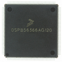
DSPB56366AG120 Freescale Semiconductor, DSPB56366AG120 Datasheet - Page 46

DSPB56366AG120
Manufacturer Part Number
DSPB56366AG120
Description
IC DSP 24BIT AUD 120MHZ 144-LQFP
Manufacturer
Freescale Semiconductor
Series
Symphony™r
Type
Audio Processorr
Datasheet
1.DSPB56366AG120.pdf
(110 pages)
Specifications of DSPB56366AG120
Interface
Host Interface, I²C, SAI, SPI
Clock Rate
120MHz
Non-volatile Memory
ROM (240 kB)
On-chip Ram
69kB
Voltage - I/o
3.30V
Voltage - Core
3.30V
Operating Temperature
-40°C ~ 110°C
Mounting Type
Surface Mount
Package / Case
144-LQFP
Lead Free Status / RoHS Status
Lead free / RoHS Compliant
Available stocks
Company
Part Number
Manufacturer
Quantity
Price
Company:
Part Number:
DSPB56366AG120
Manufacturer:
TOSHIBA
Quantity:
639
Company:
Part Number:
DSPB56366AG120
Manufacturer:
FREESCAL
Quantity:
273
Company:
Part Number:
DSPB56366AG120
Manufacturer:
Freescale Semiconductor
Quantity:
10 000
5
6
7
3-20
No.
131 Page mode cycle time for two consecutive accesses of the same
132 CAS assertion to data valid (read)
133 Column address valid to data valid (read)
134 CAS deassertion to data not valid (read hold time)
135 Last CAS assertion to RAS deassertion
136 Previous CAS deassertion to RAS deassertion
137 CAS assertion pulse width
138 Last CAS deassertion to RAS assertion
139 CAS deassertion pulse width
140 Column address valid to CAS assertion
141 CAS assertion to column address not valid
142 Last column address valid to RAS deassertion
143 WR deassertion to CAS assertion
144 CAS deassertion to WR assertion
145 CAS assertion to WR deassertion
146 WR assertion pulse width
147 Last WR assertion to RAS deassertion
148 WR assertion to CAS deassertion
149 Data valid to CAS assertion (write)
All the timings are calculated for the worst case. Some of the timings are better for specific cases (e.g., t
read-after-read or write-after-write sequences).
BRW[1:0] (DRAM Control Register bits) defines the number of wait states that should be inserted in each DRAM out-of-page
access.
RD deassertion will always occur after CAS deassertion; therefore, the restricted timing is t
direction
Page mode cycle time for mixed (read and write) accesses
• BRW[1:0] = 00
• BRW[1:0] = 01
• BRW[1:0] = 10
• BRW[1:0] = 11
Table 3-11 DRAM Page Mode Timings, Three Wait States
Characteristics
DSP56366 Technical Data, Rev. 3.1
5
Symbol
t
t
t
t
RHCP
t
t
t
t
t
t
t
t
t
t
WCH
t
RCH
RWL
CWL
t
CAC
t
OFF
RSH
CAS
CRP
t
ASC
CAH
RCS
t
RAL
WP
PC
AA
CP
DS
2.25 × T
3.75 × T
4.75 × T
6.75 × T
1.25 × T
2.25 × T
3.75 × T
3.25 × T
0.75 × T
2.5 × T
4.5 × T
1.5 × T
2.5 × T
3.5 × T
0.5 × T
Expression
2 × T
2 × T
4 × T
3 × T
1.25 × T
T
2 × T
OFF
C
1, 2, 3
C
C
− 4.0
C
C
C
C
C
C
C
C
C
C
C
C
C
C
C
C
− 7.0
− 4.0
− 4.0
C
and not t
− 7.0
C
− 4.0
− 4.0
− 4.0
− 4.0
− 4.5
− 4.0
− 6.0
− 6.0
− 6.0
− 6.0
− 4.0
− 4.2 18.3
− 4.3 33.2
− 4.3 28.2
− 4.0
C
Freescale Semiconductor
4
40.0
35.0
21.0
41.0
16.0
41.5
61.5
11.0
21.0
36.0
30.5
PC
GZ.
Min
0.0
6.0
8.5
3.5
1.0
—
—
—
—
equals 3 × T
Max
13.0
23.0
—
—
—
—
—
—
—
—
—
—
—
—
—
—
—
—
—
—
—
—
—
Unit
C
ns
ns
ns
ns
ns
ns
ns
ns
ns
ns
ns
ns
ns
ns
ns
ns
ns
ns
ns
for


