DSPB56366AG120 Freescale Semiconductor, DSPB56366AG120 Datasheet - Page 64
DSPB56366AG120
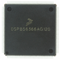
Manufacturer Part Number
DSPB56366AG120
Description
IC DSP 24BIT AUD 120MHZ 144-LQFP
Manufacturer
Freescale Semiconductor
Series
Symphony™r
Type
Audio Processorr
Datasheet
1.DSPB56366AG120.pdf
(110 pages)
Specifications of DSPB56366AG120
Interface
Host Interface, I²C, SAI, SPI
Clock Rate
120MHz
Non-volatile Memory
ROM (240 kB)
On-chip Ram
69kB
Voltage - I/o
3.30V
Voltage - Core
3.30V
Operating Temperature
-40°C ~ 110°C
Mounting Type
Surface Mount
Package / Case
144-LQFP
Lead Free Status / RoHS Status
Lead free / RoHS Compliant
Available stocks
Company
Part Number
Manufacturer
Quantity
Price
Company:

Part Number:
DSPB56366AG120
Manufacturer:
TOSHIBA
Quantity:
639
Company:
Part Number:
DSPB56366AG120
Manufacturer:
FREESCAL
Quantity:
273
Company:
Part Number:
DSPB56366AG120
Manufacturer:
Freescale Semiconductor
Quantity:
10 000


3-38
1
2
3
4
5
6
7
8
9
10
11
No.
333
334
335
336
337
338
339
340
341
342
343
344
See Host Port Usage Considerations in the DSP56366 User’s Manual.
In the timing diagrams below, the controls pins are drawn as active low. The pin polarity is programmable.
V
The read data strobe is HRD in the dual data strobe mode and HDS in the single data strobe mode.
The “last data register” is the register at address $7, which is the last location to be read or written in data transfers.
This timing is applicable only if a read from the “last data register” is followed by a read from the RXL, RXM, or RXH registers
without first polling RXDF or HREQ bits, or waiting for the assertion of the HOREQ signal.
This timing is applicable only if two consecutive reads from one of these registers are executed.
The write data strobe is HWR in the dual data strobe mode and HDS in the single data strobe mode.
The data strobe is host read (HRD) or host write (HWR) in the dual data strobe mode and host data strobe (HDS) in the single
data strobe mode.
The host request is HOREQ in the single host request mode and HRRQ and HTRQ in the double host request mode.
In this calculation, the host request signal is pulled up by a 4.7 kΩ resistor in the open-drain mode.
CC
= 3.3 V ± 0.16 V; T
HCS hold time after data strobe deassertion
Address (AD7–AD0) setup time before HAS deassertion (HMUX=1)
Address (AD7–AD0) hold time after HAS deassertion (HMUX=1)
A10–A8 (HMUX=1), A2–A0 (HMUX=0), HR/W setup time before data
strobe assertion
A10–A8 (HMUX=1), A2–A0 (HMUX=0), HR/W hold time after data strobe
deassertion
Delay from read data strobe deassertion to host request assertion for “Last
Data Register” read
Delay from write data strobe deassertion to host request assertion for “Last
Data Register” write
Delay from data strobe assertion to host request deassertion for “Last Data
Register” read or write (HROD = 0)
Delay from data strobe assertion to host request deassertion for “Last Data
Register” read or write (HROD = 1, open drain Host Request)
Delay from DMA HACK deassertion to HOREQ assertion
Delay from DMA HACK assertion to HOREQ deassertion
Delay from DMA HACK assertion to HOREQ deassertion for “Last Data
Register” read or write
• Read
• Write
•
•
• For other cases
• HROD = 0
• HROD = 1, open drain Host Request
For “Last Data Register” read
For “Last Data Register” write
9
5
9
J
= –40°C to +110°C, C
4
Table 3-18 Host Interface (HDI08) Timing
5
,
,
5
8
,
,
10
10
Characteristics
5
5
DSP56366 Technical Data, Rev. 3.1
5
,
9
,
5
10
,
L
11
= 50 pF
9
3
5
,
9
,
10
,
11
1, 2
(continued)
1.5 × T
2 × T
Expression
2 × T
C
T
—
—
—
—
—
—
—
—
—
C
C
+ 19.1
+ 19.1
C
Freescale Semiconductor
16.7
35.8
31.6
Min
0.0
4.7
3.3
4.7
3.3
8.3
0.0
—
—
—
—
0
120 MHz
300.0
300.0
Max
19.1
20.2
—
—
—
—
—
—
—
—
—
—
—
Unit
ns
ns
ns
ns
ns
ns
ns
ns
ns
ns
ns
ns
Related parts for DSPB56366AG120
Image
Part Number
Description
Manufacturer
Datasheet
Request
R

Part Number:
Description:
Manufacturer:
Freescale Semiconductor, Inc
Datasheet:
Part Number:
Description:
Manufacturer:
Freescale Semiconductor, Inc
Datasheet:
Part Number:
Description:
Manufacturer:
Freescale Semiconductor, Inc
Datasheet:
Part Number:
Description:
Manufacturer:
Freescale Semiconductor, Inc
Datasheet:
Part Number:
Description:
Manufacturer:
Freescale Semiconductor, Inc
Datasheet:
Part Number:
Description:
Manufacturer:
Freescale Semiconductor, Inc
Datasheet:
Part Number:
Description:
Manufacturer:
Freescale Semiconductor, Inc
Datasheet:
Part Number:
Description:
Manufacturer:
Freescale Semiconductor, Inc
Datasheet:
Part Number:
Description:
Manufacturer:
Freescale Semiconductor, Inc
Datasheet:
Part Number:
Description:
Manufacturer:
Freescale Semiconductor, Inc
Datasheet:
Part Number:
Description:
Manufacturer:
Freescale Semiconductor, Inc
Datasheet:
Part Number:
Description:
Manufacturer:
Freescale Semiconductor, Inc
Datasheet:
Part Number:
Description:
Manufacturer:
Freescale Semiconductor, Inc
Datasheet:
Part Number:
Description:
Manufacturer:
Freescale Semiconductor, Inc
Datasheet:
Part Number:
Description:
Manufacturer:
Freescale Semiconductor, Inc
Datasheet: