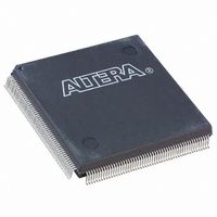
EP1K10QC208-3 Altera, EP1K10QC208-3 Datasheet - Page 29

EP1K10QC208-3
Manufacturer Part Number
EP1K10QC208-3
Description
IC ACEX 1K FPGA 10K 208-PQFP
Manufacturer
Altera
Series
ACEX-1K®r
Datasheet
1.EP1K10TC100-3N.pdf
(86 pages)
Specifications of EP1K10QC208-3
Number Of Logic Elements/cells
576
Number Of Labs/clbs
72
Total Ram Bits
12288
Number Of I /o
120
Number Of Gates
56000
Voltage - Supply
2.375 V ~ 2.625 V
Mounting Type
Surface Mount
Operating Temperature
0°C ~ 70°C
Package / Case
208-MQFP, 208-PQFP
No. Of I/o's
120
Operating Temperature Range
0°C To +70°C
Logic Case Style
QFP
No. Of Pins
208
Peak Reflow Compatible (260 C)
No
No. Of Macrocells
576
Rohs Compliant
No
Clock Management
PLL
Leaded Process Compatible
No
No. Of Gates
10000
No. Of Logic Blocks
72
Lead Free Status / RoHS Status
Contains lead / RoHS non-compliant
Other names
544-1090
Available stocks
Company
Part Number
Manufacturer
Quantity
Price
Company:
Part Number:
EP1K10QC208-3
Manufacturer:
ALTERA
Quantity:
509
Company:
Part Number:
EP1K10QC208-3
Manufacturer:
ALTERA
Quantity:
996
Part Number:
EP1K10QC208-3
Manufacturer:
ALTERA/阿尔特拉
Quantity:
20 000
Company:
Part Number:
EP1K10QC208-3N
Manufacturer:
ALTERA20
Quantity:
288
Altera Corporation
Figure 14. ACEX 1K Interconnect Resources
I/O Element (IOE)
Row
Interconnect
Column
Interconnect
IOE
IOE
IOE
IOE
LAB
LAB
B1
A1
I/O Element
An IOE contains a bidirectional I/O buffer and a register that can be used
either as an input register for external data that requires a fast setup time
or as an output register for data that requires fast clock-to-output
performance. In some cases, using an LE register for an input register will
result in a faster setup time than using an IOE register. IOEs can be used
as input, output, or bidirectional pins. The compiler uses the
programmable inversion option to invert signals from the row and
column interconnect automatically where appropriate. For bidirectional
registered I/O implementation, the output register should be in the IOE
and the data input and output enable registers should be LE registers
placed adjacent to the bidirectional pin.
I/O registers.
IOE
IOE
IOE
IOE
LAB
LAB
A2
B2
IOE
IOE
ACEX 1K Programmable Logic Device Family Data Sheet
IOE
IOE
LAB
LAB
A3
B3
IOE
IOE
IOE
IOE
Figure 15
See Figure 17
for details.
To LAB A5
To LAB A4
Carry Chains
Cascade &
To LAB B5
To LAB B4
shows the bidirectional
See Figure 16
for details.
IOE
IOE
IOE
IOE
29
13


