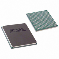
EP4CE115F29I8LN Altera, EP4CE115F29I8LN Datasheet - Page 74

EP4CE115F29I8LN
Manufacturer Part Number
EP4CE115F29I8LN
Description
IC CYCLONE IV FPGA 115K 780-FBGA
Manufacturer
Altera
Series
CYCLONE® IV Er
Datasheets
1.EP4CGX15BN11C8N.pdf
(44 pages)
2.EP4CGX15BN11C8N.pdf
(14 pages)
3.EP4CGX15BN11C8N.pdf
(478 pages)
4.EP4CGX15BN11C8N.pdf
(10 pages)
Specifications of EP4CE115F29I8LN
Number Of Logic Elements/cells
114480
Number Of Labs/clbs
7155
Total Ram Bits
3888000
Number Of I /o
528
Voltage - Supply
0.97 V ~ 1.03 V
Mounting Type
Surface Mount
Operating Temperature
-40°C ~ 100°C
Package / Case
780-FBGA
Lead Free Status / RoHS Status
Lead free / RoHS Compliant
Number Of Gates
-
Available stocks
Company
Part Number
Manufacturer
Quantity
Price
- EP4CGX15BN11C8N PDF datasheet
- EP4CGX15BN11C8N PDF datasheet #2
- EP4CGX15BN11C8N PDF datasheet #3
- EP4CGX15BN11C8N PDF datasheet #4
- Current page: 74 of 478
- Download datasheet (13Mb)
5–12
Figure 5–3. Clock Networks and Clock Control Block Locations in EP4CGX30, EP4CGX50, EP4CGX75, EP4CGX110, and
EP4CGX150 Devices
Notes to
(1) The clock networks and clock control block locations in this figure apply to only the EP4CGX30 device in F484 package and all EP4CGX50,
(2) PLL_1, PLL_2, PLL_3, and PLL_4 are general purpose PLLs while PLL_5, PLL_6, PLL_7, and PLL_8 are multipurpose PLLs.
(3) There are 6 clock control blocks on the top, right and bottom sides of the device and 12 clock control blocks on the left side of the device.
(4) REFCLK[0,1]p/n and REFCLK[4,5]p/n can only drive the general purpose PLLs and multipurpose PLLs on the left side of the device.
(5) Not available for EP4CGX30, EP4CGX50, EP4CGX75, EP4CGX110, and EP4CGX150 devices in F484 package.
(6) Dedicated clock pins can feed into this PLL. However, these paths are not fully compensated.
Cyclone IV Device Handbook, Volume 1
EP4CGX75, EP4CGX110, and EP4CGX150 devices.
These clock pins do not have access to the clock control blocks and GCLK networks. The REFCLK[4,5]p/n pins are not available in devices
in F484 package.
PLL_8
PLL_7
PLL_6
PLL_5
REFCLK[0,1]p/n (4)
HSSI
HSSI
(5)
(5)
Figure
REFCLK[4,5]p/n (4)
5–3:
3
(6)
4
(6)
4
(6)
3
(6)
(6)
(Note
PLL_2
PLL_1
(6)
2
2
1),
5
5
Clock
Control
Block (3)
Clock
Control
Block (3)
(2)
4
4
4
4
5
5
GCLK[29..0]
DPCLK[17..15]
DPCLK[2..0]
30
3
CLKIO[15..12]
CLKIO[11..8]
3
Clock
Control
Block (3)
Clock
Control
Block (3)
30
30
4
4
DPCLK[14..12]
DPCLK[5..3]
30
GCLK[29..0]
3
3
Chapter 5: Clock Networks and PLLs in Cyclone IV Devices
4
4
5
5
Clock
Control
Block (3)
(6)
(6)
5
5
© December 2010 Altera Corporation
PLL_4
PLL_3
4
4
3
3
4
Clock Networks
CLKIO[7..4]
DPCLK[11..9]
DPCLK[8..6]
Related parts for EP4CE115F29I8LN
Image
Part Number
Description
Manufacturer
Datasheet
Request
R

Part Number:
Description:
CYCLONE II STARTER KIT EP2C20N
Manufacturer:
Altera
Datasheet:

Part Number:
Description:
CPLD, EP610 Family, ECMOS Process, 300 Gates, 16 Macro Cells, 16 Reg., 16 User I/Os, 5V Supply, 35 Speed Grade, 24DIP
Manufacturer:
Altera Corporation
Datasheet:

Part Number:
Description:
CPLD, EP610 Family, ECMOS Process, 300 Gates, 16 Macro Cells, 16 Reg., 16 User I/Os, 5V Supply, 15 Speed Grade, 24DIP
Manufacturer:
Altera Corporation
Datasheet:

Part Number:
Description:
Manufacturer:
Altera Corporation
Datasheet:

Part Number:
Description:
CPLD, EP610 Family, ECMOS Process, 300 Gates, 16 Macro Cells, 16 Reg., 16 User I/Os, 5V Supply, 30 Speed Grade, 24DIP
Manufacturer:
Altera Corporation
Datasheet:

Part Number:
Description:
High-performance, low-power erasable programmable logic devices with 8 macrocells, 10ns
Manufacturer:
Altera Corporation
Datasheet:

Part Number:
Description:
High-performance, low-power erasable programmable logic devices with 8 macrocells, 7ns
Manufacturer:
Altera Corporation
Datasheet:

Part Number:
Description:
Classic EPLD
Manufacturer:
Altera Corporation
Datasheet:

Part Number:
Description:
High-performance, low-power erasable programmable logic devices with 8 macrocells, 10ns
Manufacturer:
Altera Corporation
Datasheet:

Part Number:
Description:
Manufacturer:
Altera Corporation
Datasheet:

Part Number:
Description:
Manufacturer:
Altera Corporation
Datasheet:

Part Number:
Description:
Manufacturer:
Altera Corporation
Datasheet:

Part Number:
Description:
CPLD, EP610 Family, ECMOS Process, 300 Gates, 16 Macro Cells, 16 Reg., 16 User I/Os, 5V Supply, 25 Speed Grade, 24DIP
Manufacturer:
Altera Corporation
Datasheet:


