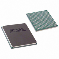
EP4CE115F29I8LN Altera, EP4CE115F29I8LN Datasheet - Page 95

EP4CE115F29I8LN
Manufacturer Part Number
EP4CE115F29I8LN
Description
IC CYCLONE IV FPGA 115K 780-FBGA
Manufacturer
Altera
Series
CYCLONE® IV Er
Datasheets
1.EP4CGX15BN11C8N.pdf
(44 pages)
2.EP4CGX15BN11C8N.pdf
(14 pages)
3.EP4CGX15BN11C8N.pdf
(478 pages)
4.EP4CGX15BN11C8N.pdf
(10 pages)
Specifications of EP4CE115F29I8LN
Number Of Logic Elements/cells
114480
Number Of Labs/clbs
7155
Total Ram Bits
3888000
Number Of I /o
528
Voltage - Supply
0.97 V ~ 1.03 V
Mounting Type
Surface Mount
Operating Temperature
-40°C ~ 100°C
Package / Case
780-FBGA
Lead Free Status / RoHS Status
Lead free / RoHS Compliant
Number Of Gates
-
Available stocks
Company
Part Number
Manufacturer
Quantity
Price
- EP4CGX15BN11C8N PDF datasheet
- EP4CGX15BN11C8N PDF datasheet #2
- EP4CGX15BN11C8N PDF datasheet #3
- EP4CGX15BN11C8N PDF datasheet #4
- Current page: 95 of 478
- Download datasheet (13Mb)
Chapter 5: Clock Networks and PLLs in Cyclone IV Devices
Phase Shift Implementation
© December 2010 Altera Corporation
Equation 5–1. Fine Resolution Phase Shift
Equation 5–1
in which f
For example, if f
depends on reference clock frequency and counter settings.
Coarse resolution phase shifts are implemented by delaying the start of the counters
for a predetermined number of counter clocks.
shift.
Equation 5–2. Coarse Resolution Phase Shift
C is the count value set for the counter delay time (this is the initial setting in the PLL
usage section of the compilation report in the Quartus II software). If the initial value
is 1, C – 1 = 0° phase shift.
Figure 5–21
VCO phase taps method. The eight phases from the VCO are shown and labeled for
reference. In this example, CLK0 is based on 0° phase from the VCO and has the C
value for the counter set to one. The CLK1 signal is divided by four, two VCO clocks
for high time and two VCO clocks for low time. CLK1 is based on the 135° phase tap
from the VCO and has the C value for the counter set to one. The CLK1 signal is also
divided by four. In this case, the two clocks are offset by 3
0° phase from the VCO but has the C value for the counter set to three. This creates a
delay of two
fine
= 156.25 ps. The PLL operating frequency defines this phase shift, a value that
REF
shows an example of phase shift insertion using fine resolution through
is the input reference clock frequency.
shows the minimum delay time that you can insert using this method.
coarse
REF
is 100 MHz, N = 1, and M = 8, then f
(two complete VCO periods).
fine
coarse
=
T
-----------
VCO
8
=
=
C 1
----------- -
f
VCO
------------- -
8f
–
VCO
1
=
Equation 5–2
=
-------------------- -
C 1
Mf
----------------- -
8Mf
–
REF
N
N
REF
VCO
Cyclone IV Device Handbook, Volume 1
= 800 MHz, and
fine
shows the coarse phase
. CLK2 is based on the
5–33
Related parts for EP4CE115F29I8LN
Image
Part Number
Description
Manufacturer
Datasheet
Request
R

Part Number:
Description:
CYCLONE II STARTER KIT EP2C20N
Manufacturer:
Altera
Datasheet:

Part Number:
Description:
CPLD, EP610 Family, ECMOS Process, 300 Gates, 16 Macro Cells, 16 Reg., 16 User I/Os, 5V Supply, 35 Speed Grade, 24DIP
Manufacturer:
Altera Corporation
Datasheet:

Part Number:
Description:
CPLD, EP610 Family, ECMOS Process, 300 Gates, 16 Macro Cells, 16 Reg., 16 User I/Os, 5V Supply, 15 Speed Grade, 24DIP
Manufacturer:
Altera Corporation
Datasheet:

Part Number:
Description:
Manufacturer:
Altera Corporation
Datasheet:

Part Number:
Description:
CPLD, EP610 Family, ECMOS Process, 300 Gates, 16 Macro Cells, 16 Reg., 16 User I/Os, 5V Supply, 30 Speed Grade, 24DIP
Manufacturer:
Altera Corporation
Datasheet:

Part Number:
Description:
High-performance, low-power erasable programmable logic devices with 8 macrocells, 10ns
Manufacturer:
Altera Corporation
Datasheet:

Part Number:
Description:
High-performance, low-power erasable programmable logic devices with 8 macrocells, 7ns
Manufacturer:
Altera Corporation
Datasheet:

Part Number:
Description:
Classic EPLD
Manufacturer:
Altera Corporation
Datasheet:

Part Number:
Description:
High-performance, low-power erasable programmable logic devices with 8 macrocells, 10ns
Manufacturer:
Altera Corporation
Datasheet:

Part Number:
Description:
Manufacturer:
Altera Corporation
Datasheet:

Part Number:
Description:
Manufacturer:
Altera Corporation
Datasheet:

Part Number:
Description:
Manufacturer:
Altera Corporation
Datasheet:

Part Number:
Description:
CPLD, EP610 Family, ECMOS Process, 300 Gates, 16 Macro Cells, 16 Reg., 16 User I/Os, 5V Supply, 25 Speed Grade, 24DIP
Manufacturer:
Altera Corporation
Datasheet:


