EZ80F920120MOD Zilog, EZ80F920120MOD Datasheet - Page 19
EZ80F920120MOD
Manufacturer Part Number
EZ80F920120MOD
Description
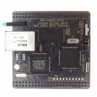
MODULE EZ80F92 512K 20MHZ
Manufacturer
Zilog
Datasheets
1.EZ80F920120MOD.pdf
(269 pages)
2.EZ80F920120MOD.pdf
(4 pages)
3.EZ80F920120MOD.pdf
(2 pages)
Specifications of EZ80F920120MOD
Module/board Type
Development Module
Processor Series
EZ80F92x
Core
eZ80
Data Bus Width
8 bit
Program Memory Type
Flash
Program Memory Size
1 MB
Interface Type
Cable
Maximum Clock Frequency
20 MHz
Operating Supply Voltage
0 V to 3.3 V
Maximum Operating Temperature
+ 70 C
Mounting Style
SMD/SMT
Package / Case
LQFP
Development Tools By Supplier
eZ80F920200ZCOG
Minimum Operating Temperature
0 C
For Use With/related Products
eZ80F92
Lead Free Status / RoHS Status
Contains lead / RoHS non-compliant
Other names
269-3157
EZ80F920120MOD
EZ80F920120MOD


Table 1. 100-Pin LQFP Pin Identification of the eZ80F92 Device (Continued)
PS015308-0404
Pin #
14
15
16
17
18
19
20
Symbol
ADDR11
ADDR12
ADDR13
ADDR14
V
V
ADDR15
DD
SS
Function
Address Bus
Address Bus
Address Bus
Address Bus
Power Supply
Ground
Address Bus
Signal Direction
Bidirectional
Bidirectional
Bidirectional
Bidirectional
Bidirectional
P R E L I M I N A R Y
Description
Configured as an output in normal
operation. The address bus selects a
location in memory or I/O space to be read
or written. Configured as an input during
bus acknowledge cycles. Drives the Chip
Select/Wait State Generator block to
generate Chip Selects.
Configured as an output in normal
operation. The address bus selects a
location in memory or I/O space to be read
or written. Configured as an input during
bus acknowledge cycles. Drives the Chip
Select/Wait State Generator block to
generate Chip Selects.
Configured as an output in normal
operation. The address bus selects a
location in memory or I/O space to be read
or written. Configured as an input during
bus acknowledge cycles. Drives the Chip
Select/Wait State Generator block to
generate Chip Selects.
Configured as an output in normal
operation. The address bus selects a
location in memory or I/O space to be read
or written. Configured as an input during
bus acknowledge cycles. Drives the Chip
Select/Wait State Generator block to
generate Chip Selects.
Power Supply.
Ground.
Configured as an output in normal
operation. The address bus selects a
location in memory or I/O space to be read
or written. Configured as an input during
bus acknowledge cycles. Drives the Chip
Select/Wait State Generator block to
generate Chip Selects.
Product Specification
eZ80F92/eZ80F93
Architectural Overview
7
Related parts for EZ80F920120MOD
Image
Part Number
Description
Manufacturer
Datasheet
Request
R

Part Number:
Description:
Communication Controllers, ZILOG INTELLIGENT PERIPHERAL CONTROLLER (ZIP)
Manufacturer:
Zilog, Inc.
Datasheet:

Part Number:
Description:
KIT DEV FOR Z8 ENCORE 16K TO 64K
Manufacturer:
Zilog
Datasheet:

Part Number:
Description:
KIT DEV Z8 ENCORE XP 28-PIN
Manufacturer:
Zilog
Datasheet:

Part Number:
Description:
DEV KIT FOR Z8 ENCORE 8K/4K
Manufacturer:
Zilog
Datasheet:

Part Number:
Description:
KIT DEV Z8 ENCORE XP 28-PIN
Manufacturer:
Zilog
Datasheet:

Part Number:
Description:
DEV KIT FOR Z8 ENCORE 4K TO 8K
Manufacturer:
Zilog
Datasheet:
Part Number:
Description:
CMOS Z8 microcontroller. ROM 16 Kbytes, RAM 256 bytes, speed 16 MHz, 32 lines I/O, 3.0V to 5.5V
Manufacturer:
Zilog, Inc.
Datasheet:
Part Number:
Description:
Low-cost microcontroller. 512 bytes ROM, 61 bytes RAM, 8 MHz
Manufacturer:
Zilog, Inc.
Datasheet:
Part Number:
Description:
Z8 4K OTP Microcontroller
Manufacturer:
Zilog, Inc.
Datasheet:
Part Number:
Description:
CMOS SUPER8 ROMLESS MCU
Manufacturer:
Zilog, Inc.
Datasheet:
Part Number:
Description:
SL1866 CMOSZ8 OTP Microcontroller
Manufacturer:
Zilog, Inc.
Datasheet:
Part Number:
Description:
SL1866 CMOSZ8 OTP Microcontroller
Manufacturer:
Zilog, Inc.
Datasheet:
Part Number:
Description:
OTP (KB) = 1, RAM = 125, Speed = 12, I/O = 14, 8-bit Timers = 2, Comm Interfaces Other Features = Por, LV Protect, Voltage = 4.5-5.5V
Manufacturer:
Zilog, Inc.
Datasheet:
Part Number:
Description:
Manufacturer:
Zilog, Inc.
Datasheet: