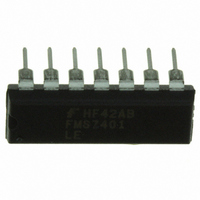
FMS7401LEN14 Fairchild Semiconductor, FMS7401LEN14 Datasheet - Page 28

FMS7401LEN14
Manufacturer Part Number
FMS7401LEN14
Description
IC CTRLR POWER DGTL EEPROM 14DIP
Manufacturer
Fairchild Semiconductor
Datasheet
1.FMS7401LVN.pdf
(81 pages)
Specifications of FMS7401LEN14
Applications
Digital Power Controller
Core Processor
8-Bit
Program Memory Type
EEPROM (1 kB)
Ram Size
64 x 8
Number Of I /o
8
Voltage - Supply
2.7 V ~ 3.6 V
Operating Temperature
-40°C ~ 85°C
Mounting Type
Through Hole
Package / Case
14-DIP (0.300", 7.62mm)
Output Current
5 mA
Input Voltage
2.7 V to 3.6 V
Switching Frequency
2 MHz
Operating Temperature Range
- 40 C to + 85 C
Mounting Style
Through Hole
Lead Free Status / RoHS Status
Lead free / RoHS Compliant
Interface
-
Controller Series
-
Lead Free Status / Rohs Status
Lead free / RoHS Compliant
Other names
FMS7401LEN14_NL
FMS7401LEN14_NL
FMS7401LEN14_NL
Available stocks
Company
Part Number
Manufacturer
Quantity
Price
Company:
Part Number:
FMS7401LEN14
Manufacturer:
Rohm
Quantity:
21 626
FMS7401L
Table 10. Programmable Comparator Upper Voltage Reference V
5.2
The Programmable Comparator circuit is configured to compare the G4/AIN0 or G2/AIN2 non-inverting input against the out-
put of the Uncommitted (Error) Amplifier (A
rent loop control, the inner (current) loop is performed by comparing the level on the G4/AIN0 or G2/AIN2 input against the
voltage present at the Uncommitted (Error) Amplifier (A
control by detecting the error signal and driving the current control loop to modify the PWM duty cycle (see
FMS7401L voltage/current loop configuration can be used in SMPS applications where the digital loop control does not have
the required accuracy and speed. Refer to the
tion details.
When VLOOP=1, the comparator output (C
input stays above A
voltage falls below A
(EPWM=0), the C
following
28
Level
32
33
34
35
36
37
38
39
40
41
42
43
44
45
46
47
48
49
50
51
52
53
54
55
56
57
58
59
60
61
62
63
Hardware Voltage and Current Loop Control (VLOOP=1)
Digital Delay Filter with PWMOFF Output
CL[5]
OUT
OUT
1
1
1
1
1
1
1
1
1
1
1
1
1
1
1
1
1
1
1
1
1
1
1
1
1
1
1
1
1
1
1
1
OUT
signal is monitored for its rising edge to generate the PWMOFF signal. Refer to
, the C
or if the Programmable Comparator circuit is disabled. If the digital delay filter circuit is enabled
OUT
CL[4]
signal will hold its state. The C
0
0
0
0
0
0
0
0
0
0
0
0
0
0
0
0
1
1
1
1
1
1
1
1
1
1
1
1
1
1
1
1
OUT
OUT
ADC Circuit
CL[3]
) is 1 when the G4/AIN0 or G2/AIN2 input pin rises above A
0
0
0
0
0
0
0
0
1
1
1
1
1
1
1
1
0
0
0
0
0
0
0
0
1
1
1
1
1
1
1
1
) when configured in a voltage/current loop control mode. In the voltage/cur-
section for addition details.
OUT
section of the datasheet for the Uncommitted Amplifier configura-
CL[2]
). The Uncommitted Amplifier performs the outer (voltage) loop
0
0
0
0
1
1
1
1
0
0
0
0
1
1
1
1
0
0
0
0
1
1
1
1
0
0
0
0
1
1
1
1
OUT
signal will equal zero if the G4/AIN0 or G2/AIN2 input
CL[1]
THU
0
0
1
1
0
0
1
1
0
0
1
1
0
0
1
1
0
0
1
1
0
0
1
1
0
0
1
1
0
0
1
1
(Levels 32 – 63)
CL[0]
0
1
0
1
0
1
0
1
0
1
0
1
0
1
0
1
0
1
0
1
0
1
0
1
0
1
0
1
0
1
0
1
PRODUCT SPECIFICATION
Voltage Reference
Figure 9
REV. 1.0.3 1/24/05
OUT
0.46V
0.51V
0.56V
0.61V
0.66V
0.71V
0.76V
0.81V
0.86V
0.91V
0.96V
1.01V
1.06V
1.11V
1.16V
1.21V
1.27V
1.32V
1.37V
1.43V
1.48V
1.53V
1.58V
1.63V
1.68V
1.73V
1.78V
1.83V
1.88V
1.94V
1.99V
2.04V
Figure
. As long as the
and the
9). The


