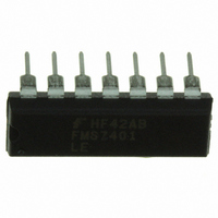
FMS7401LEN14 Fairchild Semiconductor, FMS7401LEN14 Datasheet - Page 59

FMS7401LEN14
Manufacturer Part Number
FMS7401LEN14
Description
IC CTRLR POWER DGTL EEPROM 14DIP
Manufacturer
Fairchild Semiconductor
Datasheet
1.FMS7401LVN.pdf
(81 pages)
Specifications of FMS7401LEN14
Applications
Digital Power Controller
Core Processor
8-Bit
Program Memory Type
EEPROM (1 kB)
Ram Size
64 x 8
Number Of I /o
8
Voltage - Supply
2.7 V ~ 3.6 V
Operating Temperature
-40°C ~ 85°C
Mounting Type
Through Hole
Package / Case
14-DIP (0.300", 7.62mm)
Output Current
5 mA
Input Voltage
2.7 V to 3.6 V
Switching Frequency
2 MHz
Operating Temperature Range
- 40 C to + 85 C
Mounting Style
Through Hole
Lead Free Status / RoHS Status
Lead free / RoHS Compliant
Interface
-
Controller Series
-
Lead Free Status / Rohs Status
Lead free / RoHS Compliant
Other names
FMS7401LEN14_NL
FMS7401LEN14_NL
FMS7401LEN14_NL
Available stocks
Company
Part Number
Manufacturer
Quantity
Price
Company:
Part Number:
FMS7401LEN14
Manufacturer:
Rohm
Quantity:
21 626
FMS7401L
12 In-circuit Programming Specification
The FMS7401L supports in-circuit programming of all internal memory mapped registers including the data EEPROM, code
EEPROM, and initialization registers. In-circuit programming consists of a 4-wire serial interface used to place the device in pro-
gramming mode and issue all programming commands.
ure 18
Table 32. Programming Interface Electrical Characteristics
12.1 Programming Mode Interface
In order to place the device in programming mode, a 10-bit opcode (0x34B) must be shifted into the device during its system
reset. A system reset may be triggered during the device power-up by the Power-on Reset circuit or with the device already
powered with a low pulse on the device RESET pin.
before the system reset sequence completes. If the correct opcode is shifted, the device will automatically enter programming
mode once the system reset sequence has completed.
The 10-bit opcode is serially shifted with the most significant bit (MSB) first into the device through the SHIFT_IN pin. Each
opcode data bit must be valid by T
compared against 0x34B. If the 10-bit pattern is a match, the device will set the program mode flag and the device will enter
programming mode once the system reset sequence completes (see
59
T
T
LOAD1
LOAD3
Symbol
T
T
T
and the timing rules defined by the parameters listed in
ACCESS
T
T
T
T
READY
RESET
T
T
DOS
DOH
, T
DIH
DIS
, T
LO
HI
LOAD2
LOAD4
SHIFT_OUT
SHIFT_IN
,
CLOCK
GND
FMS7401L 8-Pin PDIP/SOIC
CLOCK high time
CLOCK low time
SHIFT_IN setup time
SHIFT_IN hold time
SHIFT_OUT setup time
SHIFT_OUT hold time
SHIFT_OUT sample time
Loading time
EEPROM write time
System Reset time
1
2
3
4
Parameter
DIS
Figure 18. Programming Mode Pin Configurations
before the rising edge of CLOCK. As the opcode is shifted, the current 10-bit pattern is
8
7
6
5
SHIFT_OUT
SHIFT_IN
FMS7401L 14-Pin PDIP/SOIC/TSSOP
CLOCK
VCC
NC/VCC
NC
LOAD
GND
NC
NC
NC
3
1
After power-up, the external programmer must shift in the 10-bit opcode
The external programmer should follow the device pinout
1
2
3
4
5
6
7
Conditions
Table 31
25 °C
25 °C
25 °C
25 °C
25 °C
25 °C
25 °C
25 °C
25 °C
25 °C
13
14
12
11
10
Figure
9
8
as shown in
2
SHIFT_IN
NC/VCC
RESET
VCC
NC/VCC
NC/VCC
NC
LOAD
NC/GND
GND
VCC
19).
Min.
FMS7401L 8-Pin TSSOP
500
500
100
100
100
900
500
5
Figure 19
1
2
3
4
Typ.
and
3.7
3.7
Figure
8
7
6
5
PRODUCT SPECIFICATION
NC
LOAD
CLOCK
SHIFT_OUT
20.
Max.
DC
DC
DC
REV. 1.0.3 1/24/05
1
defined in
Units
mS
mS
nS
nS
nS
nS
nS
nS
nS
µS
Fig-


