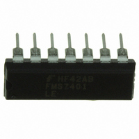
FMS7401LEN14 Fairchild Semiconductor, FMS7401LEN14 Datasheet - Page 34

FMS7401LEN14
Manufacturer Part Number
FMS7401LEN14
Description
IC CTRLR POWER DGTL EEPROM 14DIP
Manufacturer
Fairchild Semiconductor
Datasheet
1.FMS7401LVN.pdf
(81 pages)
Specifications of FMS7401LEN14
Applications
Digital Power Controller
Core Processor
8-Bit
Program Memory Type
EEPROM (1 kB)
Ram Size
64 x 8
Number Of I /o
8
Voltage - Supply
2.7 V ~ 3.6 V
Operating Temperature
-40°C ~ 85°C
Mounting Type
Through Hole
Package / Case
14-DIP (0.300", 7.62mm)
Output Current
5 mA
Input Voltage
2.7 V to 3.6 V
Switching Frequency
2 MHz
Operating Temperature Range
- 40 C to + 85 C
Mounting Style
Through Hole
Lead Free Status / RoHS Status
Lead free / RoHS Compliant
Interface
-
Controller Series
-
Lead Free Status / Rohs Status
Lead free / RoHS Compliant
Other names
FMS7401LEN14_NL
FMS7401LEN14_NL
FMS7401LEN14_NL
Available stocks
Company
Part Number
Manufacturer
Quantity
Price
Company:
Part Number:
FMS7401LEN14
Manufacturer:
Rohm
Quantity:
21 626
FMS7401L
Table 14. Timer 1 Prescale Selection (PS) Bits
6.1.2 PWM Cycle Configuration Registers
The PWM Timer 1 circuit has three 12-bit (T1CMPA, T1CMPB, T1RA) and one 5-bit (DTIME) configuration registers used to
specify the duty cycle and period of the Timer 1 output signals. Upon a system reset, all four registers are initialized with ones
(0xFFF, 0x1F). All configuration registers must be programmed with their appropriate values prior to enabling the Timer 1
circuit. Except for the DTIME register, the T1CMPA, T1CMPB and T1RA registers may be changed by software at any time;
however, if the Timer 1 circuit is in run mode, the register values will not change the Timer 1 output signal’s attributes until
after the TMR1 counter overflows ending the current PWM cycle. The last register values at the TMR1 counter overflow will
dictate the output signal’s attributes for the next PWM cycle. When reading the registers, the value reported will be the last
value written by software and may not necessarily reflect the output signal’s attributes for the current PWM cycle.
The 12-bit T1RA is Timer 1’s reload/capture register (depending on the selected operating mode). All 12 bits are accessible by
software through the 4-bit T1RAHI and 8-bit T1RALO memory mapped registers where T1RA= {T1RAHI, T1RALO}.
PWM Mode, T1RA configures the period of the T1HS1, T1HS2 and ADSTROBE outputs and determines after what TMR1
count it will overflow (reinitialize to 0x000) to begin the next PWM cycle. In Input Capture Mode, T1RA contains the captured
value of the TMR1 count at the time of the trigger defined by the rising or falling edge of the T1HS2 input.
The 12-bit T1CMPA is Timer 1’s Compare A register that dictates the length of the resting (off) state of the T1HS1 and T1HS2
output signals. All 12 bits are accessible by software through the 4-bit T1CMPAHI and 8-bit T1CMPALO memory mapped
registers where T1CMPA={T1CMPAHI, T1CMPALO}.
(TMR1=T1CMPA) to determine when the first transition of the T1HS1 and T1HS2 output signals should be triggered. In Input
Capture Mode, the T1CMPA value is still used to configure T1HS1 but has no affect on the T1HS2 signal since it is used as an
input of the Timer 1 circuit in this mode. Software must ensure that the total T1CMPA plus T
to the total T1RA plus T
The 12-bit T1CMPB is Timer 1’s Compare B register that dictates the length of the resting (off) state of the ADSTROBE out-
put signal. All 12 bits are accessible by software through the 4-bit T1CMPBHI and 8-bit T1CMPBLO memory mapped regis-
ters where T1CMPB={T1CMPBHI, T1CMPBLO}.
first transition of the ADSTROBE output signal should be triggered. If enabled, at the rising edge of ADSTROBE
(TMR1=T1CMPB) an Analog-to-Digital Converter (ADC) conversion may be initiated.
T1CMPB plus T
Bits 4-0 (DT[4:0]) of the DTIME register determines the amount of dead time (T
T1HS2 output signal transitions (see
signal transitions ending its resting (off) state. The dead time delay counter is then initiated incrementing with each edge of the
F
(off) state. As the TMR1 counter continues, once the TMR1 counter equals the T1RA value, the T1HS2 signal transitions end-
ing its active (on) state. The dead time delay counter is then reinitiated incrementing to the DT[4:0] value. Once T
passed, the T1HS1 signal will then transition ending its active (on) state.
34
T1CLK
up to the programmed DT[4:0] value.
PS[2]
0
0
0
0
1
1
1
1
DT
time is not greater than or equal to the total T1RA plus T
DT
times.
Table
PS[1]
0
0
1
1
0
0
1
1
13). In PWM Mode, once the TMR1 counter equals the T1CMPA value, the T1HS1
5
Once T
1
The TMR1 counter is compared against T1CMPB to determine when the
DT
1
has passed, the T1HS2 signal will then transition ending its resting
In PWM Mode, the TMR1 counter is compared against T1CMPA
PS[0]
0
1
0
1
0
1
0
1
DT
times.
DT
) delay, if any, between the T1HS1 and
4
Software must ensure that the total
DT
time is not greater than or equal
Timer 1 Clock
F
F
F
F
F
F
F
F
PRODUCT SPECIFICATION
T1CLK
T1CLK
T1CLK
T1CLK
T1CLK
T1CLK
T1CLK
T1CLK
/ 1
/ 2
/ 3
/ 4
/ 5
/ 6
/ 7
/ 8
REV. 1.0.3 1/24/05
DT
has
1
In


