MPC8343VRAGDB Freescale Semiconductor, MPC8343VRAGDB Datasheet - Page 11
MPC8343VRAGDB
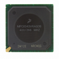
Manufacturer Part Number
MPC8343VRAGDB
Description
IC MPU POWERQUICC II 620-PBGA
Manufacturer
Freescale Semiconductor
Series
PowerQUICC II PROr
Datasheet
1.MPC8343VRAGDB.pdf
(79 pages)
Specifications of MPC8343VRAGDB
Processor Type
MPC83xx PowerQUICC II Pro 32-Bit
Speed
400MHz
Voltage
1.2V
Mounting Type
Surface Mount
Package / Case
620-PBGA
Processor Series
MPC8xxx
Core
e300
Data Bus Width
32 bit
Development Tools By Supplier
MPC8349E-MITXE
Maximum Clock Frequency
400 MHz
Maximum Operating Temperature
+ 105 C
Mounting Style
SMD/SMT
I/o Voltage
1.8 V, 2.5 V, 3.3 V
Minimum Operating Temperature
0 C
Core Size
32 Bit
Program Memory Size
64KB
Cpu Speed
400MHz
Embedded Interface Type
I2C, SPI, USB, UART
Digital Ic Case Style
BGA
No. Of Pins
620
Rohs Compliant
Yes
Family Name
MPC83xx
Device Core
PowerQUICC II Pro
Device Core Size
32b
Frequency (max)
400MHz
Instruction Set Architecture
RISC
Supply Voltage 1 (typ)
1.2V
Operating Supply Voltage (max)
1.26V
Operating Supply Voltage (min)
1.14V
Operating Temp Range
0C to 105C
Operating Temperature Classification
Commercial
Mounting
Surface Mount
Pin Count
620
Package Type
BGA
For Use With
CWH-PPC-8343N-VX - KIT EVAL SYSTEM QUICCSTART 8248CWH-PPC-8343N-VE - EVALUATION SYSTEM QUICC MPC8343E
Lead Free Status / RoHS Status
Lead free / RoHS Compliant
Features
-
Lead Free Status / Rohs Status
Lead free / RoHS Compliant
Available stocks
Company
Part Number
Manufacturer
Quantity
Price
Company:

Part Number:
MPC8343VRAGDB
Manufacturer:
Freescale Semiconductor
Quantity:
135
Company:
Part Number:
MPC8343VRAGDB
Manufacturer:
Freescale Semiconductor
Quantity:
10 000
Part Number:
MPC8343VRAGDB
Manufacturer:
FREESCALE
Quantity:
20 000


4
This section provides the clock input DC and AC electrical characteristics for the device.
4.1
Table 6
4.2
The primary clock source for the MPC8343EA can be one of two inputs, CLKIN or PCI_CLK, depending
on whether the device is configured in PCI host or PCI agent mode.
(CLKIN/PCI_CLK) AC timing specifications for the device.
Freescale Semiconductor
TSEC I/O
load = 25 pF
USB
Other I/O
Input high voltage
Input low voltage
CLKIN input current
PCI_SYNC_IN input current
PCI_SYNC_IN input current
CLKIN/PCI_CLK frequency
CLKIN/PCI_CLK cycle time
CLKIN/PCI_CLK rise and fall time
Interface
Clock Input Timing
provides the clock input (CLKIN/PCI_SYNC_IN) DC timing specifications for the MPC8343EA.
Parameter
DC Electrical Characteristics
AC Electrical Characteristics
MPC8343EA PowerQUICC II Pro Integrated Host Processor Hardware Specifications, Rev. 10
Parameter/Condition
MII
GMII or TBI
RGMII or RTBI
12 MHz
480 MHz
Parameter
Table 5. MPC8343EA Typical I/O Power Dissipation (continued)
OV
0.5 V ≤V
Table 7. CLKIN AC
Table 6. CLKIN DC Timing Specifications
DD
(1.8 V)
DDR2
GV
0 V ≤ V
0 V ≤ V
—
—
—
—
—
—
– 0.5 V ≤ V
DD
Condition
IN
IN
≤ OV
IN
—
—
≤ 0.5 V or
≤ OV
(2.5 V)
DDR1
GV
DD
—
—
—
—
—
—
IN
DD
Symbol
t
– 0.5 V
f
KH
DD
≤ OV
t
CLKIN
CLKIN
, t
Timing Specifications
KL
DD
(3.3 V)
OV
0.01
0.01
0.2
DD
Symbol
Min
0.6
15
—
V
V
I
I
I
(3.3 V)
IN
IN
IN
IH
LV
IL
0.01
0.06
—
—
—
—
DD
Table 7
Typical
1.0
—
—
(2.5 V)
LV
0.04
—
—
—
—
—
–0.3
Min
2.7
DD
—
—
—
provides the clock input
Max
2.3
66
—
Unit
W
W
W
W
W
W
OV
DD
Max
Multiply by number
of interfaces used.
±10
±10
±50
0.4
MHz
Unit
+ 0.3
Clock Input Timing
ns
ns
Comments
—
—
—
Notes
Unit
1, 6
μA
μA
μA
—
V
V
2
11
Related parts for MPC8343VRAGDB
Image
Part Number
Description
Manufacturer
Datasheet
Request
R

Part Number:
Description:
Manufacturer:
Freescale Semiconductor, Inc
Datasheet:
Part Number:
Description:
Manufacturer:
Freescale Semiconductor, Inc
Datasheet:
Part Number:
Description:
Manufacturer:
Freescale Semiconductor, Inc
Datasheet:
Part Number:
Description:
Manufacturer:
Freescale Semiconductor, Inc
Datasheet:
Part Number:
Description:
Manufacturer:
Freescale Semiconductor, Inc
Datasheet:
Part Number:
Description:
Manufacturer:
Freescale Semiconductor, Inc
Datasheet:
Part Number:
Description:
Manufacturer:
Freescale Semiconductor, Inc
Datasheet:
Part Number:
Description:
Manufacturer:
Freescale Semiconductor, Inc
Datasheet:
Part Number:
Description:
Manufacturer:
Freescale Semiconductor, Inc
Datasheet:
Part Number:
Description:
Manufacturer:
Freescale Semiconductor, Inc
Datasheet:
Part Number:
Description:
Manufacturer:
Freescale Semiconductor, Inc
Datasheet:
Part Number:
Description:
Manufacturer:
Freescale Semiconductor, Inc
Datasheet:
Part Number:
Description:
Manufacturer:
Freescale Semiconductor, Inc
Datasheet:
Part Number:
Description:
Manufacturer:
Freescale Semiconductor, Inc
Datasheet:
Part Number:
Description:
Manufacturer:
Freescale Semiconductor, Inc
Datasheet: